- 您现在的位置:买卖IC网 > PDF目录11652 > AD9992BBCZ (Analog Devices Inc)IC CCD SGNL PROC 12BIT 105CSPBGA PDF资料下载
参数资料
| 型号: | AD9992BBCZ |
| 厂商: | Analog Devices Inc |
| 文件页数: | 51/92页 |
| 文件大小: | 0K |
| 描述: | IC CCD SGNL PROC 12BIT 105CSPBGA |
| 产品变化通告: | AD9992 Discontinuation 22/Feb/2012 |
| 标准包装: | 1 |
| 类型: | CCD 信号处理器,12 位 |
| 输入类型: | 逻辑 |
| 输出类型: | 逻辑 |
| 接口: | 3 线串口 |
| 电流 - 电源: | 27mA |
| 安装类型: | 表面贴装 |
| 封装/外壳: | 105-LFBGA,CSPBGA |
| 供应商设备封装: | 105-CSPBGA(8x8) |
| 包装: | 托盘 |
第1页第2页第3页第4页第5页第6页第7页第8页第9页第10页第11页第12页第13页第14页第15页第16页第17页第18页第19页第20页第21页第22页第23页第24页第25页第26页第27页第28页第29页第30页第31页第32页第33页第34页第35页第36页第37页第38页第39页第40页第41页第42页第43页第44页第45页第46页第47页第48页第49页第50页当前第51页第52页第53页第54页第55页第56页第57页第58页第59页第60页第61页第62页第63页第64页第65页第66页第67页第68页第69页第70页第71页第72页第73页第74页第75页第76页第77页第78页第79页第80页第81页第82页第83页第84页第85页第86页第87页第88页第89页第90页第91页第92页
AD9992
Rev. C | Page 55 of 92
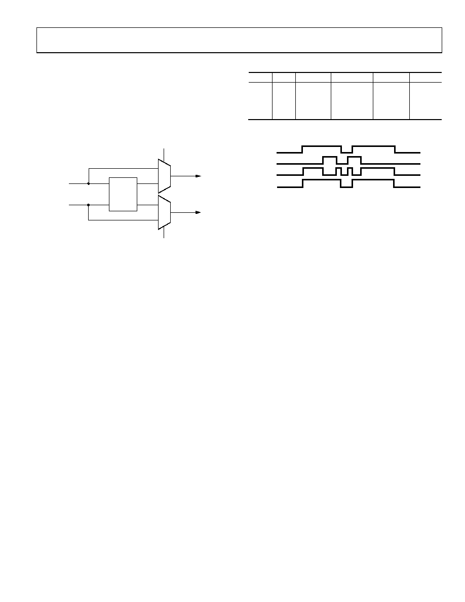
GP LOOK-UP TABLES (LUT)
The AD9992 is equipped with a look-up table for each pair of
consecutive GP signals when configured as outputs. GP1 is
always combined with GP2, GP3 is always combined with GP4,
GP5 is always combined with GP6, and GP7 is always combined
with GP8. The external GPO outputs from each pair can output
the result of the LUT or the original GP internal signal.
GP1
LUT
1
0
1
GPO2
GPO1
GP2
GP2_USE_LUT
GP1_USE_LUT
05
89
1-
06
4
Figure 63. Internal LUT for GP1 and GP2 Signals
Address 0x79 dictates the behavior of the LUT and which
signals receive the result. Each 4-bit LUT_FOR_GPxy register
can realize any logic combination of GPx and GPy. For example,
Table 24 shows how the register values of LUT_FOR_GP12 [11:8]
are determined. XOR, NAND, AND, and OR results are shown,
but any 4-bit combination is possible. A simple example of XOR
gating is shown in Figure 64.
Table 24. LUT Results Based on GP1 and GP2 Values
GP2
GP1
LUT: XOR
LUT: NAND
LUT: AND
LUT: OR
0
1
0
1
0
1
0
1
0
1
0
1
GP1
GP2
GPO2
NOTES
1. LOGIC COMBINATION (XOR) OF PROGRAMMED TOGGLES
GP1 AND GP2.
LUT_FOR_GP12[11:8] = 0x06
GP2_USE_LUT = 1
GP1_USE_LUT = 0
GPO1
0
589
1-
0
65
Figure 64. LUT Example for GP1 XOR GP2
Field Counter and GPO Limitations
The following is a summary of the known limitations of the field
counters and GPO signals that dictate usability:
The field counter trigger (PRIMARY_ACTION and
SECONDARY_ACTION registers, Address 0x70) is self-reset
at the start of every VD period. Therefore, there must be one
VD period between sequential programming to that address.
If GP*_PROTOCOL = 1, it must be manually reset to
GP*_PROTOCOL = 0 one VD period before it can be used
again. If manual toggles are desired in sequential fields, the
MANUAL_TRIG register should be used in conjunction with
GP*_PROTOCOL = 1.
相关PDF资料 |
PDF描述 |
|---|---|
| VI-JN3-IY-F1 | CONVERTER MOD DC/DC 24V 50W |
| VI-JN2-IZ-B1 | CONVERTER MOD DC/DC 15V 25W |
| VI-JN2-IY-F4 | CONVERTER MOD DC/DC 15V 50W |
| VI-JN2-IY-F3 | CONVERTER MOD DC/DC 15V 50W |
| AD22050NZ | IC AMP DIFF SGL SUPPLY 8-DIP |
相关代理商/技术参数 |
参数描述 |
|---|---|
| AD9992BBCZRL | 功能描述:IC CCD SGNL PROC 12BIT 105CSPBGA RoHS:是 类别:集成电路 (IC) >> 接口 - 传感器和探测器接口 系列:- 其它有关文件:Automotive Product Guide 产品培训模块:Lead (SnPb) Finish for COTS Obsolescence Mitigation Program 标准包装:74 系列:- 类型:触控式传感器 输入类型:数字 输出类型:数字 接口:JTAG,串行 电流 - 电源:100µA 安装类型:表面贴装 封装/外壳:20-TSSOP(0.173",4.40mm 宽) 供应商设备封装:20-TSSOP 包装:管件 |
| AD9993BBCZ | 功能描述:IC MIXED-SIGNAL FRONT END 196BGA 制造商:analog devices inc. 系列:- 包装:托盘 零件状态:在售 类型:ADC,DAC 输入类型:LVDS 输出类型:LVDS 接口:SPI 电流 - 电源:- 工作温度:- 安装类型:表面贴装 封装/外壳:196-LFBGA,CSPBGA 供应商器件封装:196-CSPBGA(12x12) 标准包装:1 |
| AD9993BBCZRL | 功能描述:IC MIXED-SIGNAL FRONT END 196BGA 制造商:analog devices inc. 系列:- 包装:带卷(TR) 零件状态:在售 类型:ADC,DAC 输入类型:LVDS 输出类型:LVDS 接口:SPI 电流 - 电源:- 工作温度:- 安装类型:表面贴装 封装/外壳:196-LFBGA,CSPBGA 供应商器件封装:196-CSPBGA(12x12) 标准包装:1,500 |
| AD9993-EBZ | 功能描述:EVAL BOARD MXFE AD9993 制造商:analog devices inc. 系列:* 零件状态:在售 标准包装:1 |
| AD9994 | 制造商:AD 制造商全称:Analog Devices 功能描述:12-Bit CCD Signal Processor with Precision Timing Generator |
发布紧急采购,3分钟左右您将得到回复。