- 您现在的位置:买卖IC网 > PDF目录170341 > CXA3266Q PHASE LOCKED LOOP, 0.12 MHz, PQFP48 PDF资料下载
参数资料
| 型号: | CXA3266Q |
| 元件分类: | PLL合成/DDS/VCOs |
| 英文描述: | PHASE LOCKED LOOP, 0.12 MHz, PQFP48 |
| 封装: | PLASTIC, QFP-48 |
| 文件页数: | 13/62页 |
| 文件大小: | 929K |
| 代理商: | CXA3266Q |
第1页第2页第3页第4页第5页第6页第7页第8页第9页第10页第11页第12页当前第13页第14页第15页第16页第17页第18页第19页第20页第21页第22页第23页第24页第25页第26页第27页第28页第29页第30页第31页第32页第33页第34页第35页第36页第37页第38页第39页第40页第41页第42页第43页第44页第45页第46页第47页第48页第49页第50页第51页第52页第53页第54页第55页第56页第57页第58页第59页第60页第61页第62页
CXA3266Q
- 20 -
Delay Sync Output
The front edge of the delay sync pulse is latched by the pulse obtained by frequency dividing the CLK
regenerated by the PLL, so there is almost no jitter with respect to CLK. This front edge can be used as the
reset signal for the system timing circuit.
The rear edge of the delay sync pulse is latched by the CLK regenerated by the PLL. This relationship is
undefined for one clock as shown in the Timing Chart.
The delay sync output delay time can be varied in two stages. First, the delay time can be varied in the range
of 8/32 to 48/32 CLK using 6 bits of control register, and then in the range of 2 to 5 CLK using 2 bits of control
register. In other words, the total delay time is ((8/32 to 48/32) + (2 to 5)) CLK. (See the I/O Timing Chart.)
DSYNC output is TTL and PECL (complementary), and supports both positive and negative polarity. Clock TTL
output can also be turned off.
Programmable Counter TTL Output Switching
Output (PECL, TTL) from DSYNC output is possible by switching of control register.
Delay Sync Output Width (DSYNC By-pass = 0)
Delay sync output pulse width can be varied to 1, 2, 4, or 8CLK by switching 2 bits of control register.
Delay Sync Output Delay (DSYNC By-pass = 0)
DIVOUT output delay from delay sync output can be varied to 4CLK or 5CLK by switching of control register.
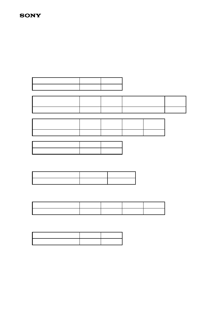
Register : Clock Enable
1
0
Clock output status
ON
OFF
Lower delay line
FINE DELAY bits 0 to 5
000111
001000
101111
Delay time
8/32CLK
9/32CLK
48/32CLK
Upper delay line
COARSE DELAY bits 0 to 1
00
01
10
11
Delay time
2CLK
3CLK
4CLK
5CLK
Register : DSYNC POL
1
0
DSYNC output polarity
Positive
Negative
Register : DSYNC By-pass
0
1
Output status from DSYNC
DIVOUT output
DSYNC output
Register : DSYNC WIDTH
00
01
10
11
DSYNC width
1CLK
2CLK
4CLK
8CLK
Register : DSYNC DELAY
0
1
Delay time
4CLK
5CLK
相关PDF资料 |
PDF描述 |
|---|---|
| CXA3621GE | SPECIALTY ANALOG CIRCUIT, PBGA30 |
| CXB1140Q | 1000 SERIES, LOW LEVEL TRIGGERED D LATCH, COMPLEMENTARY OUTPUT, MQFP32 |
| CXK77B3640GB-4 | 128K X 36 LATE-WRITE SRAM, 5.3 ns, PBGA119 |
| CXK77P18L80AGB-4A | 512K X 18 LATE-WRITE SRAM, 3.8 ns, PBGA119 |
| CXO-199-148.5MHZ | CRYSTAL OSCILLATOR, SINE OUTPUT, 148.5 MHz |
相关代理商/技术参数 |
参数描述 |
|---|---|
| CXA3268AR | 制造商:SONY 制造商全称:Sony Corporation 功能描述:Driver/Timing Generator for Color LCD Panels |
| CXA3271AGE | 制造商:未知厂家 制造商全称:未知厂家 功能描述:Fingerprint Sensor |
| CXA3271GE | 制造商:SONY 制造商全称:Sony Corporation 功能描述:Fingerprint Sensor |
| CXA3272R | 制造商:SONY 制造商全称:Sony Corporation 功能描述:CXA3272R |
| CXA3275Q | 制造商:SONY 制造商全称:Sony Corporation 功能描述:PLL/OSC/MIX IC for Digital Tuner |
发布紧急采购,3分钟左右您将得到回复。