- 您现在的位置:买卖IC网 > PDF目录170341 > CXA3266Q PHASE LOCKED LOOP, 0.12 MHz, PQFP48 PDF资料下载
参数资料
| 型号: | CXA3266Q |
| 元件分类: | PLL合成/DDS/VCOs |
| 英文描述: | PHASE LOCKED LOOP, 0.12 MHz, PQFP48 |
| 封装: | PLASTIC, QFP-48 |
| 文件页数: | 30/62页 |
| 文件大小: | 929K |
| 代理商: | CXA3266Q |
第1页第2页第3页第4页第5页第6页第7页第8页第9页第10页第11页第12页第13页第14页第15页第16页第17页第18页第19页第20页第21页第22页第23页第24页第25页第26页第27页第28页第29页当前第30页第31页第32页第33页第34页第35页第36页第37页第38页第39页第40页第41页第42页第43页第44页第45页第46页第47页第48页第49页第50页第51页第52页第53页第54页第55页第56页第57页第58页第59页第60页第61页第62页
CXA3266Q
- 36 -
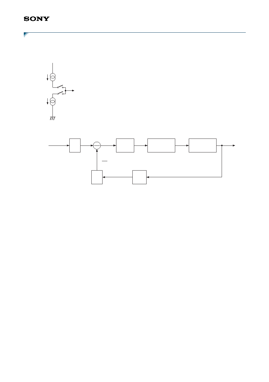
Charge Pump and Loop Filter Settings
The CXA3266Q's charge pump is a constant-current output type as shown below.
The PLL closed loop transmittance is obtained by the following formula.
(
θo/N)/θr = (KPD F (S) KVCO 1/N 1/S)/(1 + KPD F (S) KVCO 1/N 1/S) ... (1)
Here, KPD, F (S), and KVCO are ;
*1
The reason for the 1/S inside the phase detector is as follows.
θo (t)/N =
0
(t)/Ndt +
θo (t = 0)/N... (a)
If
θo (t = 0) = 0,
θo (t)/N =
0
(t)/Ndt... (b)
Performing Laplace conversion ;
θo (S)/N = 1/s W0 (S)/N... (c)
When a constant-current output charge pump circuit is used inside the PLL, the
phase detector output acts as a current source, and the dimension of its
transmittance KPD is A/rad. Also, when considering the VCO input as a voltage,
the LPF transmittance dimension must be expressed in ohms (
= V/A).
Therefore, the PLL transmittance when a constant-current output charge pump
circuit is used is as follows.
KPD
: Phase comparator gain
(A/rad)
F (S)
: Loop filter transmittance
(
)
KVCO
: VCO gain
(rad/sV)
S1
S2
To LPF
VCC
1/S
KPD
(A/rad)
F (S)
()
KVCO
(rad/sV)
1/S
1/N
PD
LPF
VCO
counter
o
N
0
0/N
r
+
–
ω
θ
ω
o
t
∫
ω
o
t
∫
相关PDF资料 |
PDF描述 |
|---|---|
| CXA3621GE | SPECIALTY ANALOG CIRCUIT, PBGA30 |
| CXB1140Q | 1000 SERIES, LOW LEVEL TRIGGERED D LATCH, COMPLEMENTARY OUTPUT, MQFP32 |
| CXK77B3640GB-4 | 128K X 36 LATE-WRITE SRAM, 5.3 ns, PBGA119 |
| CXK77P18L80AGB-4A | 512K X 18 LATE-WRITE SRAM, 3.8 ns, PBGA119 |
| CXO-199-148.5MHZ | CRYSTAL OSCILLATOR, SINE OUTPUT, 148.5 MHz |
相关代理商/技术参数 |
参数描述 |
|---|---|
| CXA3268AR | 制造商:SONY 制造商全称:Sony Corporation 功能描述:Driver/Timing Generator for Color LCD Panels |
| CXA3271AGE | 制造商:未知厂家 制造商全称:未知厂家 功能描述:Fingerprint Sensor |
| CXA3271GE | 制造商:SONY 制造商全称:Sony Corporation 功能描述:Fingerprint Sensor |
| CXA3272R | 制造商:SONY 制造商全称:Sony Corporation 功能描述:CXA3272R |
| CXA3275Q | 制造商:SONY 制造商全称:Sony Corporation 功能描述:PLL/OSC/MIX IC for Digital Tuner |
发布紧急采购,3分钟左右您将得到回复。