- 您现在的位置:买卖IC网 > PDF目录170341 > CXA3266Q PHASE LOCKED LOOP, 0.12 MHz, PQFP48 PDF资料下载
参数资料
| 型号: | CXA3266Q |
| 元件分类: | PLL合成/DDS/VCOs |
| 英文描述: | PHASE LOCKED LOOP, 0.12 MHz, PQFP48 |
| 封装: | PLASTIC, QFP-48 |
| 文件页数: | 29/62页 |
| 文件大小: | 929K |
| 代理商: | CXA3266Q |
第1页第2页第3页第4页第5页第6页第7页第8页第9页第10页第11页第12页第13页第14页第15页第16页第17页第18页第19页第20页第21页第22页第23页第24页第25页第26页第27页第28页当前第29页第30页第31页第32页第33页第34页第35页第36页第37页第38页第39页第40页第41页第42页第43页第44页第45页第46页第47页第48页第49页第50页第51页第52页第53页第54页第55页第56页第57页第58页第59页第60页第61页第62页
CXA3266Q
- 35 -
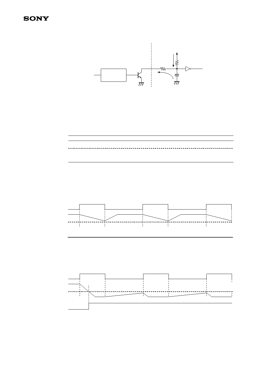
UNLOCK Timing
The unlock detect output is an open collector. When unlock detect output S1 goes High, the current I1 is pulled in.
The UNLOCK sensitivity can be adjusted by connecting external resistors (R1, R2) and a capacitor (C) to this
output pin appropriately and changing these values. Operation during three modes is described below.
CASE 1 : When there is no phase difference, that is to say, when the PLL is locked.
The S1 signal is Low and the S2 signal is High.
The UNLOCK output remains Low.
CASE 2 : When there is a phase difference, that is to say, when the S1 signal goes High and Low as shown in
the figure below, the fall slew rate of the S2 signal is determined by the current I1 flowing into that open
collector. Therefore, increasing the resistance R1 causes the S2 signal fall slew rate to become slower.
Also, since the S2 signal rise slew rate is determined by the current I2, reducing the resistance R2
causes the S2 signal rise slew rate to become faster. If this integrated S2 signal does not fall below the
threshold level of the next inverter, the UNLOCK signal stays Low, and the PLL is said to be locked.
CASE 3 : However, even if a phase difference exists as shown above, if the resistance R1 is reduced, the
current I1 flowing into the open collector increases, and the S2 signal fall slew rate becomes faster.
Also, if the resistance R2 is increased, the S2 signal rise slew rate becomes slower. If this integrated
S2 signal falls below the threshold level of the next inverter, the UNLOCK signal goes from Low to
High, and the PLL is said to be unlocked.
unlock
detect
UNLOCK
VCC
Signal from
phase comparator
C
R1
R2
S2
I2
I1
S1
Outside the IC
Inside the IC
S1
S2
UNLOCK
threshold
level
S1
S2
UNLOCK
threshold
level
S1
S2
UNLOCK
threshold
level
相关PDF资料 |
PDF描述 |
|---|---|
| CXA3621GE | SPECIALTY ANALOG CIRCUIT, PBGA30 |
| CXB1140Q | 1000 SERIES, LOW LEVEL TRIGGERED D LATCH, COMPLEMENTARY OUTPUT, MQFP32 |
| CXK77B3640GB-4 | 128K X 36 LATE-WRITE SRAM, 5.3 ns, PBGA119 |
| CXK77P18L80AGB-4A | 512K X 18 LATE-WRITE SRAM, 3.8 ns, PBGA119 |
| CXO-199-148.5MHZ | CRYSTAL OSCILLATOR, SINE OUTPUT, 148.5 MHz |
相关代理商/技术参数 |
参数描述 |
|---|---|
| CXA3268AR | 制造商:SONY 制造商全称:Sony Corporation 功能描述:Driver/Timing Generator for Color LCD Panels |
| CXA3271AGE | 制造商:未知厂家 制造商全称:未知厂家 功能描述:Fingerprint Sensor |
| CXA3271GE | 制造商:SONY 制造商全称:Sony Corporation 功能描述:Fingerprint Sensor |
| CXA3272R | 制造商:SONY 制造商全称:Sony Corporation 功能描述:CXA3272R |
| CXA3275Q | 制造商:SONY 制造商全称:Sony Corporation 功能描述:PLL/OSC/MIX IC for Digital Tuner |
发布紧急采购,3分钟左右您将得到回复。