- 您现在的位置:买卖IC网 > PDF目录170341 > CXA3266Q PHASE LOCKED LOOP, 0.12 MHz, PQFP48 PDF资料下载
参数资料
| 型号: | CXA3266Q |
| 元件分类: | PLL合成/DDS/VCOs |
| 英文描述: | PHASE LOCKED LOOP, 0.12 MHz, PQFP48 |
| 封装: | PLASTIC, QFP-48 |
| 文件页数: | 17/62页 |
| 文件大小: | 929K |
| 代理商: | CXA3266Q |
第1页第2页第3页第4页第5页第6页第7页第8页第9页第10页第11页第12页第13页第14页第15页第16页当前第17页第18页第19页第20页第21页第22页第23页第24页第25页第26页第27页第28页第29页第30页第31页第32页第33页第34页第35页第36页第37页第38页第39页第40页第41页第42页第43页第44页第45页第46页第47页第48页第49页第50页第51页第52页第53页第54页第55页第56页第57页第58页第59页第60页第61页第62页
CXA3266Q
- 24 -
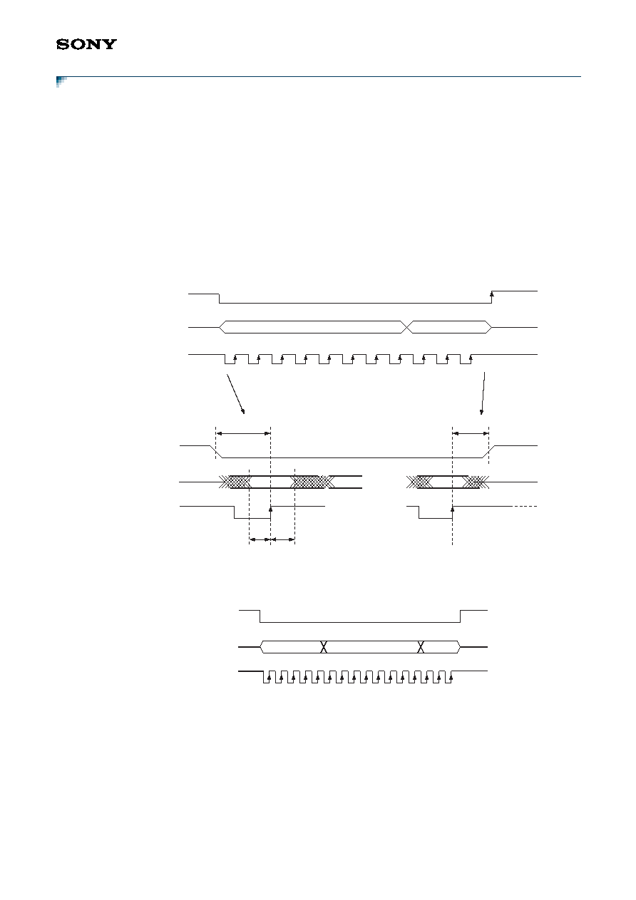
Control Register Timing
Write Mode
Many functions of the CXA3266Q can be controlled via a program. Characteristics are changed by setting the
internal control register values via a serial interface comprised of three pins : SENABLE (Pin 10), SCLK (Pin 11)
and SDATA (Pin 12). The write timing diagram is shown below.
Input the 8-bit data and 3-bit register address MSB first to the SDATA pin. Some registers are not 8 bits, but
the data is input aligned with the LSB side in these cases. (See the Register Table.)
SENABLE is the enable signal and is active Low. SCLK is the transfer clock signal, and data is loaded to the IC
at the rising edge. When SENABLE rises, SCLK must be High. (Registers are set at the rising edge of SENABLE.)
When SENABLE falls, SCLK may be either High or Low.
For example, when inputting a 16-bit signal, the initial 5 bits are invalid and the latter 11 bits are valid. That is
to say, the latter 11 bits are loaded to the register.
SENABLE
SDATA
SCLK
SENABLE
SDATA
SCLK
DATA
8 bits
ADDRESS
3 bits
Enlarged
TENS
TENH
TDH
TDS
SENABLE
SDATA
SCLK
DATA
8 bits
address
3 bits
Invalid DATA
5 bits
相关PDF资料 |
PDF描述 |
|---|---|
| CXA3621GE | SPECIALTY ANALOG CIRCUIT, PBGA30 |
| CXB1140Q | 1000 SERIES, LOW LEVEL TRIGGERED D LATCH, COMPLEMENTARY OUTPUT, MQFP32 |
| CXK77B3640GB-4 | 128K X 36 LATE-WRITE SRAM, 5.3 ns, PBGA119 |
| CXK77P18L80AGB-4A | 512K X 18 LATE-WRITE SRAM, 3.8 ns, PBGA119 |
| CXO-199-148.5MHZ | CRYSTAL OSCILLATOR, SINE OUTPUT, 148.5 MHz |
相关代理商/技术参数 |
参数描述 |
|---|---|
| CXA3268AR | 制造商:SONY 制造商全称:Sony Corporation 功能描述:Driver/Timing Generator for Color LCD Panels |
| CXA3271AGE | 制造商:未知厂家 制造商全称:未知厂家 功能描述:Fingerprint Sensor |
| CXA3271GE | 制造商:SONY 制造商全称:Sony Corporation 功能描述:Fingerprint Sensor |
| CXA3272R | 制造商:SONY 制造商全称:Sony Corporation 功能描述:CXA3272R |
| CXA3275Q | 制造商:SONY 制造商全称:Sony Corporation 功能描述:PLL/OSC/MIX IC for Digital Tuner |
发布紧急采购,3分钟左右您将得到回复。