- 您现在的位置:买卖IC网 > PDF目录385639 > MT48LC1M16A1S (Micron Technology, Inc.) SYNCHRONOUS DRAM PDF资料下载
参数资料
| 型号: | MT48LC1M16A1S |
| 厂商: | Micron Technology, Inc. |
| 英文描述: | SYNCHRONOUS DRAM |
| 中文描述: | 同步DRAM |
| 文件页数: | 16/51页 |
| 文件大小: | 1480K |
| 代理商: | MT48LC1M16A1S |
第1页第2页第3页第4页第5页第6页第7页第8页第9页第10页第11页第12页第13页第14页第15页当前第16页第17页第18页第19页第20页第21页第22页第23页第24页第25页第26页第27页第28页第29页第30页第31页第32页第33页第34页第35页第36页第37页第38页第39页第40页第41页第42页第43页第44页第45页第46页第47页第48页第49页第50页第51页
16Mb: x16 SDRAM
16MSDRAMx16.p65
–
Rev. 8/99
Micron Technology, Inc., reserves the right to change products or specifications without notice.
1999, Micron Technology, Inc.
16
16Mb: x16
SDRAM
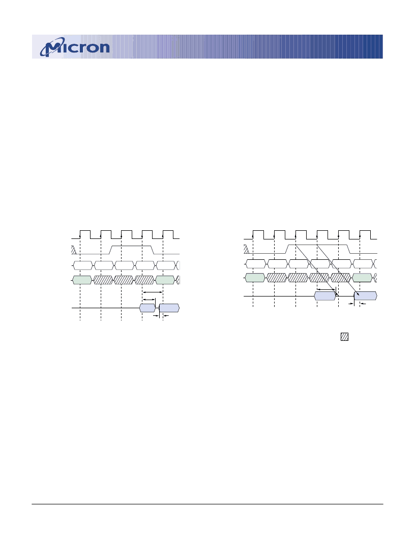
Data from any READ burst may be truncated with
a subsequent WRITE command, and data from a
fixed-length READ burst may be immediately followed
by data from a subsequent WRITE command (subject
to bus turnaround limitations). The WRITE burst may
be initiated on the clock edge immediately following
the last (or last desired) data element from the READ
burst, provided that I/O contention can be avoided. In
a given system design, there may be the possibility that
the device driving the input data would go Low-Z
before the SDRAM DQs go High-Z. In this case, at least
a single-cycle delay should occur between the last read
data and the WRITE command.
The DQM input is used to avoid I/O contention as
shown in Figures 9 and 10. The DQM signal must be
asserted (HIGH) at least two clocks (DQM latency is
two clocks for output buffers) prior to the WRITE
DON
’
T CARE
READ
NOP
NOP
NOP
NOP
DQM
CLK
DQ
D
OUT
n
T2
T1
T4
T3
T0
COMMAND
ADDRESS
BANK,
COL
n
WRITE
D
IN
b
BANK,
COL
b
T5
DS
t
HZ
t
NOTE:
A CAS latency of three is used for illustration. The
READ command
may be to any bank, and the WRITE command may be to any bank.
Figure 10
READ to WRITE w ith
Extra Clock Cycle
Figure 9
READ to WRITE
READ
NOP
NOP
WRITE
NOP
CLK
T2
T1
T4
T3
T0
DQM
DQ
D
OUT
n
COMMAND
D
IN
b
ADDRESS
BANK,
COL
n
BANK,
COL
b
DS
t
HZ
t
t
CK
NOTE:
A CAS latency of three is used for illustration. The
READ
command may be to any bank, and the WRITE command
may be to any bank. If a burst of one is used, then DQM is
not required.
command to suppress data-out from the READ. Once
the WRITE command is registered, the DQs will go
High-Z (or remain High-Z) regardless of the state of the
DQM signal, provided the DQM was active on the
clock just prior to the WRITE command that truncated
the READ command. If not, the second WRITE will be
an invalid WRITE. For example, if DQM was LOW
during T4 in Figure 10, then the WRITEs at T5 and T7
would be valid, while the WRITE at T6 would be
invalid.
The DQM signal must be de-asserted (DQM latency
is zero clocks for input buffers) prior to the WRITE
command to ensure that the written data is not masked.
Figure 9 shows the case where the clock frequency
allows for bus contention to be avoided without add-
ing a NOP cycle, and Figure 10 shows the case where the
additional NOP is needed.
相关PDF资料 |
PDF描述 |
|---|---|
| MT48LC2M32LFFC | 512K x 32 x 4 banks 3.3v SDRAM(3.3V,512K x 32 x 4组同步动态RAM) |
| MT48LC4M16A2 | SYNCHRONOUS DRAM |
| MT48LC16M4A2 | RSD Series - Econoline Unregulated DC-DC Converters; Input Voltage (Vdc): 24V; Output Voltage (Vdc): 3.3V; Power: 1W; 1kVDC and 3kVDC Isolation Options; Approved for Medical Applications; Suitable for Automated Assembly; 8, 10 and 12 pin Pinning Style Options; Optional Continuous Short Circuit Protected; Efficiency to 85% |
| MT48LC8M16A2 | SYNCHRONOUS DRAM |
| MT48V2M32LFFC | 512K x 32 x 4 banks 2.5V SDRAM(2.5V,512K x 32 x 4组同步动态RAM) |
相关代理商/技术参数 |
参数描述 |
|---|---|
| MT48LC1M16A1-TG | 制造商:Micron Technology Inc 功能描述: |
| MT48LC1M16A1TG6SE | 制造商:MICRON 功能描述:New |
| MT48LC1M16A1TG-6SE | 制造商:Micron Technology Inc 功能描述:IC,SDRAM,2X512KX16,CMOS,TSOP,50PIN,PLASTIC |
| MT48LC1M16A1TG-7S | 制造商:Mitel Networks Corporation 功能描述:SDRAM, 1M x 16, 50 Pin, Plastic, TSOP |
| MT48LC1M16A1TG-7SE | 制造商:Micron Technology Inc 功能描述:SDRAM, 1M x 16, 50 Pin, Plastic, TSOP |
发布紧急采购,3分钟左右您将得到回复。