- 您现在的位置:买卖IC网 > PDF目录385639 > MT48LC1M16A1S (Micron Technology, Inc.) SYNCHRONOUS DRAM PDF资料下载
参数资料
| 型号: | MT48LC1M16A1S |
| 厂商: | Micron Technology, Inc. |
| 英文描述: | SYNCHRONOUS DRAM |
| 中文描述: | 同步DRAM |
| 文件页数: | 19/51页 |
| 文件大小: | 1480K |
| 代理商: | MT48LC1M16A1S |
第1页第2页第3页第4页第5页第6页第7页第8页第9页第10页第11页第12页第13页第14页第15页第16页第17页第18页当前第19页第20页第21页第22页第23页第24页第25页第26页第27页第28页第29页第30页第31页第32页第33页第34页第35页第36页第37页第38页第39页第40页第41页第42页第43页第44页第45页第46页第47页第48页第49页第50页第51页
16Mb: x16 SDRAM
16MSDRAMx16.p65
–
Rev. 8/99
Micron Technology, Inc., reserves the right to change products or specifications without notice.
1999, Micron Technology, Inc.
19
16Mb: x16
SDRAM
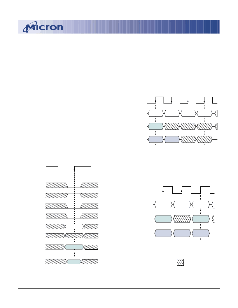
WRITEs
WRITE bursts are initiated with a WRITE com-
mand, as shown in Figure 13.
The starting column and bank addresses are pro-
vided with the WRITE command and AUTO
PRECHARGE is either enabled or disabled for that
access. If AUTO PRECHARGE is enabled, the row being
accessed is precharged at the completion of the burst.
For the generic WRITE commands used in the follow-
ing illustrations, AUTO PRECHARGE is disabled.
During WRITE bursts, the first valid data-in element
will be registered coincident with the WRITE com-
mand. Subsequent data elements will be registered on
each successive positive clock edge. Upon completion
of a fixed-length burst, assuming no other commands
have been initiated, the DQs will remain High-Z, and
any additional input data will be ignored (see Figure
14). A full-page burst will continue until terminated.
(At the end of the page it will wrap to column 0 and
continue.)
Data for any WRITE burst may be truncated with a
subsequent WRITE command, and data for a fixed-
length WRITE burst may be immediately followed by
data for a subsequent WRITE command. The new
WRITE command can be issued on any clock following
the previous WRITE command, and the data provided
Figure 15
WRITE to WRITE
coincident with the new command applies to the new
command. An example is shown in Figure 15. Data
n
+ 1 is either the last of a burst of two, or the last desired
of a longer burst. The 1 Meg x 16 SDRAM uses a
pipelined architecture and therefore does not require
the 2
n
rule associated with a prefetch architecture.
A WRITE command can be initiated on any clock cycle
following a previous WRITE command. Full-speed,
CLK
DQ
D
IN
n
T2
T1
T3
T0
COMMAND
ADDRESS
NOP
NOP
WRITE
D
IN
n
+ 1
NOP
BANK,
COL
n
NOTE:
Burst length = 2. DQM is LOW.
Figure 14
WRITE Burst
DON
’
T CARE
CLK
DQ
T2
T1
T0
COMMAND
ADDRESS
NOP
WRITE
WRITE
BANK,
COL
n
BANK,
COL
b
D
IN
n
D
IN
n
+ 1
D
IN
b
NOTE:
DQM is LOW.
Each WRITE
command may be to any bank.
CS#
WE#
CAS#
RAS#
CKE
CLK
COLUMN
A0-A7
A10
BA
BANK 0
BANK 1
HIGH
ENABLE AUTO PRECHARGE
DISABLE AUTO PRECHARGE
A8-A9
Figure 13
WRITE Command
相关PDF资料 |
PDF描述 |
|---|---|
| MT48LC2M32LFFC | 512K x 32 x 4 banks 3.3v SDRAM(3.3V,512K x 32 x 4组同步动态RAM) |
| MT48LC4M16A2 | SYNCHRONOUS DRAM |
| MT48LC16M4A2 | RSD Series - Econoline Unregulated DC-DC Converters; Input Voltage (Vdc): 24V; Output Voltage (Vdc): 3.3V; Power: 1W; 1kVDC and 3kVDC Isolation Options; Approved for Medical Applications; Suitable for Automated Assembly; 8, 10 and 12 pin Pinning Style Options; Optional Continuous Short Circuit Protected; Efficiency to 85% |
| MT48LC8M16A2 | SYNCHRONOUS DRAM |
| MT48V2M32LFFC | 512K x 32 x 4 banks 2.5V SDRAM(2.5V,512K x 32 x 4组同步动态RAM) |
相关代理商/技术参数 |
参数描述 |
|---|---|
| MT48LC1M16A1-TG | 制造商:Micron Technology Inc 功能描述: |
| MT48LC1M16A1TG6SE | 制造商:MICRON 功能描述:New |
| MT48LC1M16A1TG-6SE | 制造商:Micron Technology Inc 功能描述:IC,SDRAM,2X512KX16,CMOS,TSOP,50PIN,PLASTIC |
| MT48LC1M16A1TG-7S | 制造商:Mitel Networks Corporation 功能描述:SDRAM, 1M x 16, 50 Pin, Plastic, TSOP |
| MT48LC1M16A1TG-7SE | 制造商:Micron Technology Inc 功能描述:SDRAM, 1M x 16, 50 Pin, Plastic, TSOP |
发布紧急采购,3分钟左右您将得到回复。