- 您现在的位置:买卖IC网 > PDF目录69322 > RK80546KG0802MM (INTEL CORP) 64-BIT, 3000 MHz, MICROPROCESSOR, CPGA604 PDF资料下载
参数资料
| 型号: | RK80546KG0802MM |
| 厂商: | INTEL CORP |
| 元件分类: | 微控制器/微处理器 |
| 英文描述: | 64-BIT, 3000 MHz, MICROPROCESSOR, CPGA604 |
| 封装: | FLIP CHIP, MICRO PGA-604 |
| 文件页数: | 57/106页 |
| 文件大小: | 4724K |
| 代理商: | RK80546KG0802MM |
第1页第2页第3页第4页第5页第6页第7页第8页第9页第10页第11页第12页第13页第14页第15页第16页第17页第18页第19页第20页第21页第22页第23页第24页第25页第26页第27页第28页第29页第30页第31页第32页第33页第34页第35页第36页第37页第38页第39页第40页第41页第42页第43页第44页第45页第46页第47页第48页第49页第50页第51页第52页第53页第54页第55页第56页当前第57页第58页第59页第60页第61页第62页第63页第64页第65页第66页第67页第68页第69页第70页第71页第72页第73页第74页第75页第76页第77页第78页第79页第80页第81页第82页第83页第84页第85页第86页第87页第88页第89页第90页第91页第92页第93页第94页第95页第96页第97页第98页第99页第100页第101页第102页第103页第104页第105页第106页
54
Datasheet
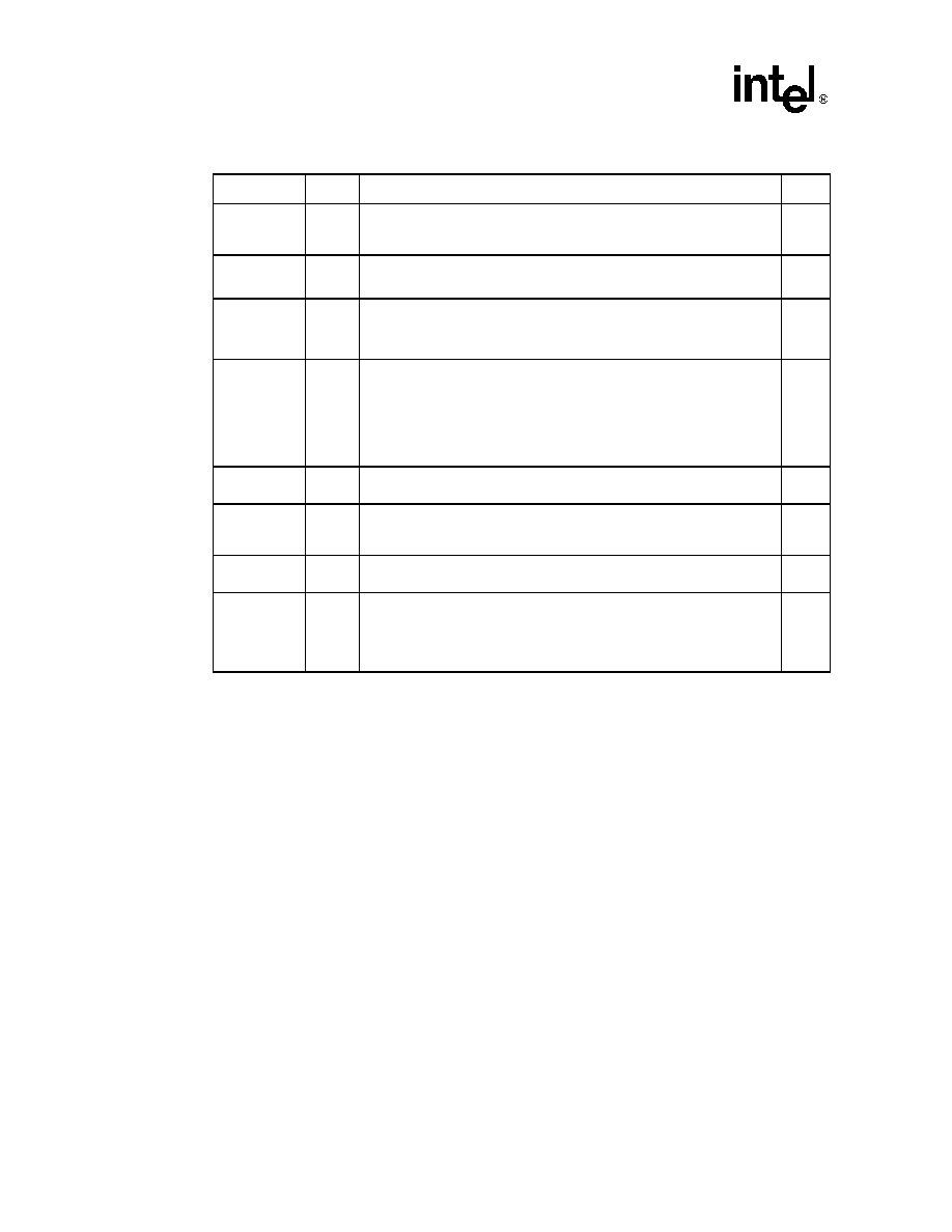
Signal Definitions
NOTES:
1. The 64-bit Intel Xeon processor with 2 MB L2 cache only supports BR0# and BR1#. However, platforms
must terminate BR2# and BR3# to VTT.
2. For this pin on the 64-bit Intel Xeon processor with 2 MB L2 cache, the maximum number of symmetric
agents is one. Maximum number of central agents is zero.
3. For this pin on the 64-bit Intel Xeon processor with 2 MB L2 cache, the maximum number of symmetric
agents is two. Maximum number of central agents is zero.
4. For this pin on the 64-bit Intel Xeon processor with 2 MB L2 cache, the maximum number of symmetric
agents is two. Maximum number of central agents is one.
VCCIOPLL
I
VCCIOPLL provides isolated power for digital portion of the internal
processor core PLL’s. Refer to the appropriate platform design guidelines
for complete implementation details.
VCCPLL
I
The on-die PLL filter solution will not be implemented on this
platform. The VCCPLL input should be left unconnected.
VCCSENSE
VSSSENSE
O
VCCSENSE and VSSSENSE provide an isolated, low impedance
connection to the processor core power and ground. They can be
used to sense or measure power near the silicon with little noise.
VID[5:0]
O
VID[5:0] (Voltage ID) pins are used to support automatic selection of power
supply voltages (VCC). These are open drain signals that are driven by the
processor and must be pulled up through a resistor. Conversely, the VR
output must be disabled prior to the voltage supply for these pins becomes
invalid. The VID pins are needed to support processor voltage specification
variations. See Table 2-3 for definitions of these pins. The VR must supply
the voltage that is requested by these pins, or disable itself.
VIDPWRGD
I
The processor requires this input to determine that the supply voltage for
BSEL[1:0] and VID[5:0] is stable and within specification.
VSSA
I
VSSA provides an isolated, internal ground for internal PLL’s. Do not
connect directly to ground. This pin is to be connected to VCCA and
VCCIOPLL through a discrete filter circuit.
VTT
P
The front side bus termination voltage input pins. Refer to Table 2-8 for
further details.
VTTEN
O
The VTTEN can be used as an output enable for the VTT regulator in the
event an incompatible processor is inserted into the platform. There is no
connection to the processor silicon for this signal and it must be pulled up
through a resistor. Refer to the appropriate platform design guidelines for
implementation details.
Table 4-1. Signal Definitions (Sheet 10 of 10)
Name
Type
Description
Notes
相关PDF资料 |
PDF描述 |
|---|---|
| RK80546PG0801M | 32-BIT, 3000 MHz, MICROPROCESSOR, CPGA478 |
| RK80546PE0721M | 32-BIT, 2800 MHz, MICROPROCESSOR, CPGA478 |
| RL5C478A | PCI BUS CONTROLLER, PQFP256 |
| RM100355WFQMLV | 100K SERIES, LOW LEVEL TRIGGERED D LATCH, COMPLEMENTARY OUTPUT, CQFP24 |
| RM48L950PGET | 32-BIT, FLASH, 200 MHz, RISC MICROCONTROLLER, PQFP144 |
相关代理商/技术参数 |
参数描述 |
|---|---|
| RK80546KG0802MMS L7ZF | 制造商:Intel 功能描述:MPU Xeon NetBurst 64-Bit 90nm 3GHz 604-Pin FCmPGA4 制造商:Intel 功能描述:XEON 3E GHZ,2M,800MHZ,FC MPGA4 - Trays |
| RK80546KG0881M S L7PF | 制造商:Intel 功能描述:INTEL XEON, 3.2DGHZ,1M,800MHZ,FC-MPGA4 - Trays |
| RK80546KG0882MMS L7ZE | 制造商:Intel 功能描述:XEON 3.2,2M,800MHZ,FC-MPGA4 - Trays |
| RK80546KG1041M | 制造商:Rochester Electronics LLC 功能描述:XEON 3.6GHZ,1M,800MHZ,FC MPGA4 - Bulk |
| RK80546KG1041M S L7PH | 制造商:Intel 功能描述:MPU Xeon 制造商:Intel 功能描述:MPU XEON 90NM 3.6GHZ 604PIN PGA - Trays |
发布紧急采购,3分钟左右您将得到回复。