- 您现在的位置:买卖IC网 > PDF目录1987 > AD9520-0BCPZ-REEL7 (Analog Devices Inc)IC CLOCK GEN 2.8GHZ VCO 64LFCSP PDF资料下载
参数资料
| 型号: | AD9520-0BCPZ-REEL7 |
| 厂商: | Analog Devices Inc |
| 文件页数: | 10/80页 |
| 文件大小: | 0K |
| 描述: | IC CLOCK GEN 2.8GHZ VCO 64LFCSP |
| 设计资源: | Synchronizing Multiple AD9910 1 GSPS Direct Digital Synthesizers (CN0121) Phase Coherent FSK Modulator (CN0186) |
| 标准包装: | 750 |
| 类型: | 时钟发生器,扇出配送 |
| PLL: | 是 |
| 输入: | CMOS,LVDS,LVPECL |
| 输出: | CMOS,LVPECL |
| 电路数: | 1 |
| 比率 - 输入:输出: | 2:12,2:24 |
| 差分 - 输入:输出: | 是/是 |
| 频率 - 最大: | 2.95GHz |
| 除法器/乘法器: | 是/无 |
| 电源电压: | 3.135 V ~ 3.465 V |
| 工作温度: | -40°C ~ 85°C |
| 安装类型: | 表面贴装 |
| 封装/外壳: | 64-VFQFN 裸露焊盘,CSP |
| 供应商设备封装: | 64-LFCSP-VQ(9x9) |
| 包装: | 带卷 (TR) |
第1页第2页第3页第4页第5页第6页第7页第8页第9页当前第10页第11页第12页第13页第14页第15页第16页第17页第18页第19页第20页第21页第22页第23页第24页第25页第26页第27页第28页第29页第30页第31页第32页第33页第34页第35页第36页第37页第38页第39页第40页第41页第42页第43页第44页第45页第46页第47页第48页第49页第50页第51页第52页第53页第54页第55页第56页第57页第58页第59页第60页第61页第62页第63页第64页第65页第66页第67页第68页第69页第70页第71页第72页第73页第74页第75页第76页第77页第78页第79页第80页
AD9520-0
Data Sheet
Rev. A | Page 18 of 80
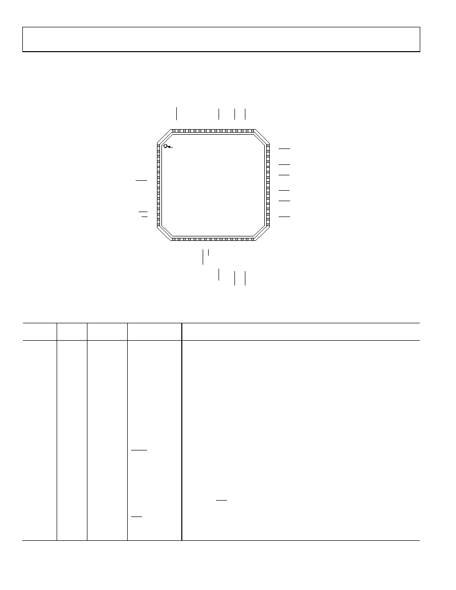
PIN CONFIGURATION AND FUNCTION DESCRIPTIONS
NOTES
1. EXPOSED DIE PAD MUST BE CONNECTED TO GND.
PIN 1
INDICATOR
17
18
19
20
21
22
23
24
25
26
27
28
29
30
31
32
S
D
IO/S
D
A
S
DO
G
ND
SP1
SP0
EEPR
O
M
R
ESET
PD
O
UT
9
(
O
UT
9A)
O
UT
9
(
O
UT
9B)
V
S
_DRV
O
UT
10
(
O
UT
10A)
O
UT
10
(
O
UT
10B)
O
UT
11
(
O
UT
11A)
O
UT
11
(
O
UT
11B)
VS
64
63
62
61
60
59
58
57
56
55
54
53
52
51
50
49
RE
F
IN
(
RE
F
1)
RE
F
IN
(
RE
F
2)
C
PR
SET
VS
G
ND
R
SET
VS
O
UT
0
(
O
UT
0A)
O
UT
0
(
O
UT
0B)
V
S
_DRV
O
UT
1
(
O
UT
1A)
O
UT
1
(
O
UT
1B)
O
UT
2
(
O
UT
2A)
O
UT
2
(
O
UT
2B)
VS
1
2
3
4
5
6
7
8
9
10
11
12
13
14
15
16
VS
REFMON
LD
VCP
CP
STATUS
REF_SEL
SYNC
LF
BYPASS
VS
CLK
CS
SCLK/SCL
OUT3 (OUT3A)
OUT3 (OUT3B)
VS_DRV
OUT4 (OUT4A)
OUT4 (OUT4B)
OUT5 (OUT5A)
OUT5 (OUT5B)
VS
OUT8 (OUT8B)
OUT8 (OUT8A)
OUT7 (OUT7B)
OUT7 (OUT7A)
VS_DRV
OUT6 (OUT6B)
OUT6 (OUT6A)
48
47
46
45
44
43
42
41
40
39
38
37
36
35
34
33
AD9520
TOP VIEW
(Not to Scale)
07213-
003
Figure 5. Pin Configuration
Table 21. Pin Function Descriptions
Pin No.
Input/
Output
Pin Type
Mnemonic
Description
1, 11, 12,
32, 40, 41,
49, 57, 60,
61
I
Power
VS
3.3 V Power Pins.
2
O
3.3 V CMOS
REFMON
Reference Monitor (Output). This pin has multiple selectable outputs.
3
O
3.3 V CMOS
LD
Lock Detect (Output). This pin has multiple selectable outputs.
4
I
Power
VCP
Power Supply for Charge Pump (CP); VS ≤ VCP ≤ 5.25 V. VCP must still be connected
to 3.3 V if the PLL is not used.
5
O
Loop filter
CP
Charge Pump (Output). This pin connects to an external loop filter; it can be left
unconnected if the PLL is not used.
6
O
3.3 V CMOS
STATUS
Programmable Status Output.
7
I
3.3 V CMOS
REF_SEL
Reference Select. This pin selects REF1 (low) or REF2 (high) and has an internal 30 k
pull-down resistor.
8
I
3.3 V CMOS
SYNC
Manual Synchronization and Manual Holdover. This pin initiates a manual
synchronization and is used for manual holdover. Active low. This pin has an
internal 30 k pull-up resistor.
9
I
Loop filter
LF
Loop Filter (Input). This pin connects internally to the VCO control voltage node.
10
O
Loop filter
BYPASS
This pin is for bypassing the LDO to ground with a 220 nF capacitor. It can be left
unconnected if the PLL is not used.
13
I
Differential
clock input
CLK
Along with CLK, this pin is the differential input for the clock distribution section.
14
I
Differential
clock input
CLK
Along with CLK, this pin is the differential input for the clock distribution section. If a
single-ended input is connected to the CLK pin, connect a 0.1 F bypass capacitor from
this pin to ground.
相关PDF资料 |
PDF描述 |
|---|---|
| AD9520-1BCPZ | IC CLOCK GEN 2.5GHZ VCO 64LFCSP |
| AD9520-2BCPZ | IC CLOCK GEN 2.2GHZ VCO 64LFCSP |
| AD9520-3BCPZ-REEL7 | IC CLOCK GEN 2GHZ VCO 64LFCSP |
| AD9520-4BCPZ-REEL7 | IC CLOCK GEN 1.6GHZ VCO 64LFCSP |
| AD9520-5BCPZ-REEL7 | IC CLOCK GEN EXT VCO 64LFCSP |
相关代理商/技术参数 |
参数描述 |
|---|---|
| AD9520-1 | 制造商:AD 制造商全称:Analog Devices 功能描述:12 LVPECL/24 CMOS Output Clock Generator with Integrated 2.5 GHz VCO |
| AD9520-1/PCBZ | 功能描述:BOARD EVAL FOR AD9520-1 RoHS:是 类别:编程器,开发系统 >> 评估演示板和套件 系列:- 标准包装:1 系列:PSoC® 主要目的:电源管理,热管理 嵌入式:- 已用 IC / 零件:- 主要属性:- 次要属性:- 已供物品:板,CD,电源 |
| AD9520-1BCPZ | 功能描述:IC CLOCK GEN 2.5GHZ VCO 64LFCSP RoHS:是 类别:集成电路 (IC) >> 时钟/计时 - 时钟发生器,PLL,频率合成器 系列:- 标准包装:2,000 系列:- 类型:PLL 时钟发生器 PLL:带旁路 输入:LVCMOS,LVPECL 输出:LVCMOS 电路数:1 比率 - 输入:输出:2:11 差分 - 输入:输出:是/无 频率 - 最大:240MHz 除法器/乘法器:是/无 电源电压:3.135 V ~ 3.465 V 工作温度:0°C ~ 70°C 安装类型:表面贴装 封装/外壳:32-LQFP 供应商设备封装:32-TQFP(7x7) 包装:带卷 (TR) |
| AD9520-1BCPZ-REEL7 | 功能描述:IC CLOCK GEN 2.5GHZ VCO 64LFCSP RoHS:是 类别:集成电路 (IC) >> 时钟/计时 - 时钟发生器,PLL,频率合成器 系列:- 标准包装:2,000 系列:- 类型:PLL 时钟发生器 PLL:带旁路 输入:LVCMOS,LVPECL 输出:LVCMOS 电路数:1 比率 - 输入:输出:2:11 差分 - 输入:输出:是/无 频率 - 最大:240MHz 除法器/乘法器:是/无 电源电压:3.135 V ~ 3.465 V 工作温度:0°C ~ 70°C 安装类型:表面贴装 封装/外壳:32-LQFP 供应商设备封装:32-TQFP(7x7) 包装:带卷 (TR) |
| AD9520-2 | 制造商:AD 制造商全称:Analog Devices 功能描述:12 LVPECL/24 CMOS Output Clock Generator with Integrated 2.2 GHz VCO |
发布紧急采购,3分钟左右您将得到回复。