- 您现在的位置:买卖IC网 > PDF目录1987 > AD9520-0BCPZ-REEL7 (Analog Devices Inc)IC CLOCK GEN 2.8GHZ VCO 64LFCSP PDF资料下载
参数资料
| 型号: | AD9520-0BCPZ-REEL7 |
| 厂商: | Analog Devices Inc |
| 文件页数: | 64/80页 |
| 文件大小: | 0K |
| 描述: | IC CLOCK GEN 2.8GHZ VCO 64LFCSP |
| 设计资源: | Synchronizing Multiple AD9910 1 GSPS Direct Digital Synthesizers (CN0121) Phase Coherent FSK Modulator (CN0186) |
| 标准包装: | 750 |
| 类型: | 时钟发生器,扇出配送 |
| PLL: | 是 |
| 输入: | CMOS,LVDS,LVPECL |
| 输出: | CMOS,LVPECL |
| 电路数: | 1 |
| 比率 - 输入:输出: | 2:12,2:24 |
| 差分 - 输入:输出: | 是/是 |
| 频率 - 最大: | 2.95GHz |
| 除法器/乘法器: | 是/无 |
| 电源电压: | 3.135 V ~ 3.465 V |
| 工作温度: | -40°C ~ 85°C |
| 安装类型: | 表面贴装 |
| 封装/外壳: | 64-VFQFN 裸露焊盘,CSP |
| 供应商设备封装: | 64-LFCSP-VQ(9x9) |
| 包装: | 带卷 (TR) |
第1页第2页第3页第4页第5页第6页第7页第8页第9页第10页第11页第12页第13页第14页第15页第16页第17页第18页第19页第20页第21页第22页第23页第24页第25页第26页第27页第28页第29页第30页第31页第32页第33页第34页第35页第36页第37页第38页第39页第40页第41页第42页第43页第44页第45页第46页第47页第48页第49页第50页第51页第52页第53页第54页第55页第56页第57页第58页第59页第60页第61页第62页第63页当前第64页第65页第66页第67页第68页第69页第70页第71页第72页第73页第74页第75页第76页第77页第78页第79页第80页
Data Sheet
AD9520-0
Rev. A | Page 67 of 80
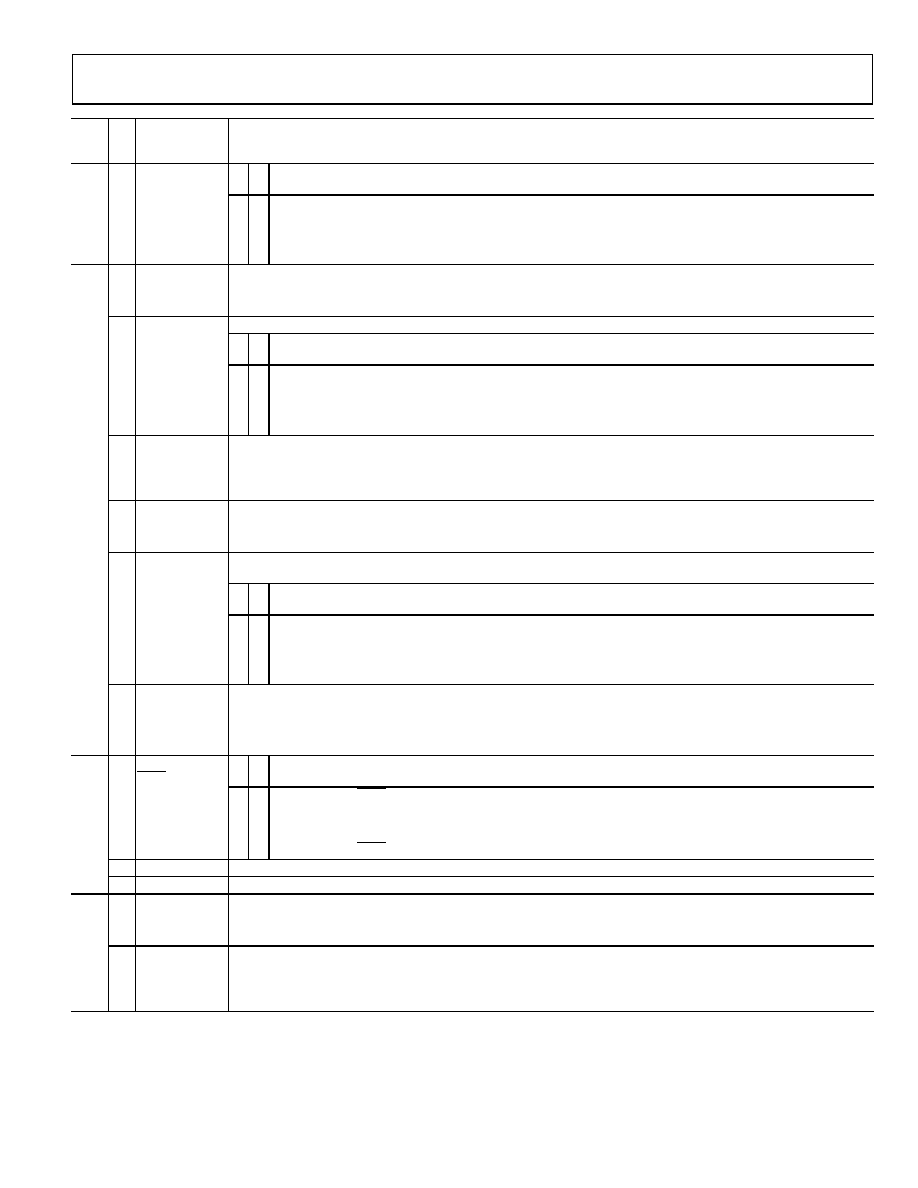
Reg.
Addr.
(Hex) Bits Name
Description
[1:0] Antibacklash
pulse width
Bit
1
Bit
0 Antibacklash Pulse Width (ns)
0
2.9 (default)
0
1
1.3
1
0
6.0
1
2.9
0x018 7
Enable CMOS
reference input
dc offset
Enables dc offset in single-ended CMOS input mode to prevent chattering when ac-coupled and input is lost.
0: disables dc offset (default).
1: enables dc offset.
[6:5] Lock detect
counter
Required consecutive number of PFD cycles with edges inside lock detect window before the DLD indicates a locked condition.
Bit
6
Bit
5 PFD Cycles to Determine Lock
0
5 (default)
0
1
16
1
0
64
1
255
4
Digital lock detect
window
If the time difference of the rising edges at the inputs to the PFD is less than the lock detect window time, the digital lock detect
flag is set. The flag remains set until the time difference is greater than the loss-of-lock threshold.
0: high range (default). The default setting is 3.5 ns.
1: low range.
3
Disable digital
lock detect
Digital lock detect operation.
0: normal lock detect operation (default).
1: disables lock detect.
[2:1] VCO calibration
divider
Divider used to generate the VCO calibration clock from the PLL reference clock (see the VCO Calibration section for the recommended
setting of the VCO calibration divider based on the PFD rate).
Bit
2
Bit
1 VCO Calibration Clock Divider
0
2. This setting is fine for PFD frequencies < 12.5 MHz. The PFD frequency is fREF/R.
0
1
4. This setting is fine for PFD frequencies < 12.5 MHz. The PFD frequency is fREF/R.
1
0
8. This setting is fine for PFD frequencies < 50 MHz.
1
16 (default). This setting is fine for any PFD frequency, but it also results in the longest VCO calibration time.
0
VCO calibration
now
Initiates VCO calibration. This bit must be toggled from 0b to 1b in the active registers. The sequence to initiate a calibration is
as follows: program to 0b, followed by an IO_UPDATE (Register 0x232[0]); then program to 1b, followed by another IO_UPDATE
(Register 0x232[0]). This sequence gives complete control over when the VCO calibration occurs relative to the programming of
other registers that can impact the calibration (default = 0b). Note that the VCO divider (Register 0x1E0[2:0]) must not be static during
VCO calibration.
0x019 [7:6] R, A, B counters
SYNC pin reset
Bit
7
Bit
6 Action
0
Does nothing on SYNC (default).
0
1
Asynchronous reset.
1
0
Synchronous reset.
1
Does nothing on SYNC.
[5:3] R path delay
R path delay, see Table 2 (default: 0x0).
[2:0] N path delay
N path delay, see Table 2 (default: 0x0).
0x01A 7
Enable STATUS
pin divider
Enables a divide-by-4 on the STATUS pin. This makes it easier to look at low duty-cycle signals out of the R and N dividers.
0: divide-by-4 disabled on STATUS pin (default).
1: divide-by-4 enabled on STATUS pin.
6
Ref freq monitor
threshold
Sets the reference (REF1/REF2) frequency monitor’s detection threshold frequency. This does not affect the VCO frequency monitor’s
detection threshold (see Table 17: REF1, REF2, and VCO frequency status monitor parameter).
0: frequency valid if frequency is above 1.02 MHz (default).
1: frequency valid if frequency is above 6 kHz.
相关PDF资料 |
PDF描述 |
|---|---|
| AD9520-1BCPZ | IC CLOCK GEN 2.5GHZ VCO 64LFCSP |
| AD9520-2BCPZ | IC CLOCK GEN 2.2GHZ VCO 64LFCSP |
| AD9520-3BCPZ-REEL7 | IC CLOCK GEN 2GHZ VCO 64LFCSP |
| AD9520-4BCPZ-REEL7 | IC CLOCK GEN 1.6GHZ VCO 64LFCSP |
| AD9520-5BCPZ-REEL7 | IC CLOCK GEN EXT VCO 64LFCSP |
相关代理商/技术参数 |
参数描述 |
|---|---|
| AD9520-1 | 制造商:AD 制造商全称:Analog Devices 功能描述:12 LVPECL/24 CMOS Output Clock Generator with Integrated 2.5 GHz VCO |
| AD9520-1/PCBZ | 功能描述:BOARD EVAL FOR AD9520-1 RoHS:是 类别:编程器,开发系统 >> 评估演示板和套件 系列:- 标准包装:1 系列:PSoC® 主要目的:电源管理,热管理 嵌入式:- 已用 IC / 零件:- 主要属性:- 次要属性:- 已供物品:板,CD,电源 |
| AD9520-1BCPZ | 功能描述:IC CLOCK GEN 2.5GHZ VCO 64LFCSP RoHS:是 类别:集成电路 (IC) >> 时钟/计时 - 时钟发生器,PLL,频率合成器 系列:- 标准包装:2,000 系列:- 类型:PLL 时钟发生器 PLL:带旁路 输入:LVCMOS,LVPECL 输出:LVCMOS 电路数:1 比率 - 输入:输出:2:11 差分 - 输入:输出:是/无 频率 - 最大:240MHz 除法器/乘法器:是/无 电源电压:3.135 V ~ 3.465 V 工作温度:0°C ~ 70°C 安装类型:表面贴装 封装/外壳:32-LQFP 供应商设备封装:32-TQFP(7x7) 包装:带卷 (TR) |
| AD9520-1BCPZ-REEL7 | 功能描述:IC CLOCK GEN 2.5GHZ VCO 64LFCSP RoHS:是 类别:集成电路 (IC) >> 时钟/计时 - 时钟发生器,PLL,频率合成器 系列:- 标准包装:2,000 系列:- 类型:PLL 时钟发生器 PLL:带旁路 输入:LVCMOS,LVPECL 输出:LVCMOS 电路数:1 比率 - 输入:输出:2:11 差分 - 输入:输出:是/无 频率 - 最大:240MHz 除法器/乘法器:是/无 电源电压:3.135 V ~ 3.465 V 工作温度:0°C ~ 70°C 安装类型:表面贴装 封装/外壳:32-LQFP 供应商设备封装:32-TQFP(7x7) 包装:带卷 (TR) |
| AD9520-2 | 制造商:AD 制造商全称:Analog Devices 功能描述:12 LVPECL/24 CMOS Output Clock Generator with Integrated 2.2 GHz VCO |
发布紧急采购,3分钟左右您将得到回复。