- 您现在的位置:买卖IC网 > PDF目录1987 > AD9520-0BCPZ-REEL7 (Analog Devices Inc)IC CLOCK GEN 2.8GHZ VCO 64LFCSP PDF资料下载
参数资料
| 型号: | AD9520-0BCPZ-REEL7 |
| 厂商: | Analog Devices Inc |
| 文件页数: | 28/80页 |
| 文件大小: | 0K |
| 描述: | IC CLOCK GEN 2.8GHZ VCO 64LFCSP |
| 设计资源: | Synchronizing Multiple AD9910 1 GSPS Direct Digital Synthesizers (CN0121) Phase Coherent FSK Modulator (CN0186) |
| 标准包装: | 750 |
| 类型: | 时钟发生器,扇出配送 |
| PLL: | 是 |
| 输入: | CMOS,LVDS,LVPECL |
| 输出: | CMOS,LVPECL |
| 电路数: | 1 |
| 比率 - 输入:输出: | 2:12,2:24 |
| 差分 - 输入:输出: | 是/是 |
| 频率 - 最大: | 2.95GHz |
| 除法器/乘法器: | 是/无 |
| 电源电压: | 3.135 V ~ 3.465 V |
| 工作温度: | -40°C ~ 85°C |
| 安装类型: | 表面贴装 |
| 封装/外壳: | 64-VFQFN 裸露焊盘,CSP |
| 供应商设备封装: | 64-LFCSP-VQ(9x9) |
| 包装: | 带卷 (TR) |
第1页第2页第3页第4页第5页第6页第7页第8页第9页第10页第11页第12页第13页第14页第15页第16页第17页第18页第19页第20页第21页第22页第23页第24页第25页第26页第27页当前第28页第29页第30页第31页第32页第33页第34页第35页第36页第37页第38页第39页第40页第41页第42页第43页第44页第45页第46页第47页第48页第49页第50页第51页第52页第53页第54页第55页第56页第57页第58页第59页第60页第61页第62页第63页第64页第65页第66页第67页第68页第69页第70页第71页第72页第73页第74页第75页第76页第77页第78页第79页第80页
AD9520-0
Data Sheet
Rev. A | Page 34 of 80
Phase-Locked Loop (PLL)
PROGRAMMABLE
N DELAY
REFIN
CLK
REF1
REF2
BUF
STATUS
R
DI
V
IDE
R
CL
O
CK
DO
UBL
E
R
STATUS
P
RO
G
RAM
M
ABL
E
R
DE
L
AY
REFERENCE
SWITCHOVER
REF_SEL
CPRSET VCP
VS
GND
RSET
DISTRIBUTION
REFERENCE
REFMON
CP
STATUS
LD
P, P + 1
PRESCALER
A/B
COUNTERS
N DIVIDER
BYPASS
LF
LOW DROPOUT
REGULATOR (LDO)
PHASE
FREQUENCY
DETECTOR
LOCK
DETECT
CHARGE
PUMP
PL
L
RE
F
E
RE
NCE
HOLD
0
1
DIVIDE BY 1,
2, 3, 4, 5, OR 6
ZERO DELAY BLOCK
FROM CHANNEL
DIVIDER 0
VS_DRV
OPTIONAL
REFIN
07213-
064
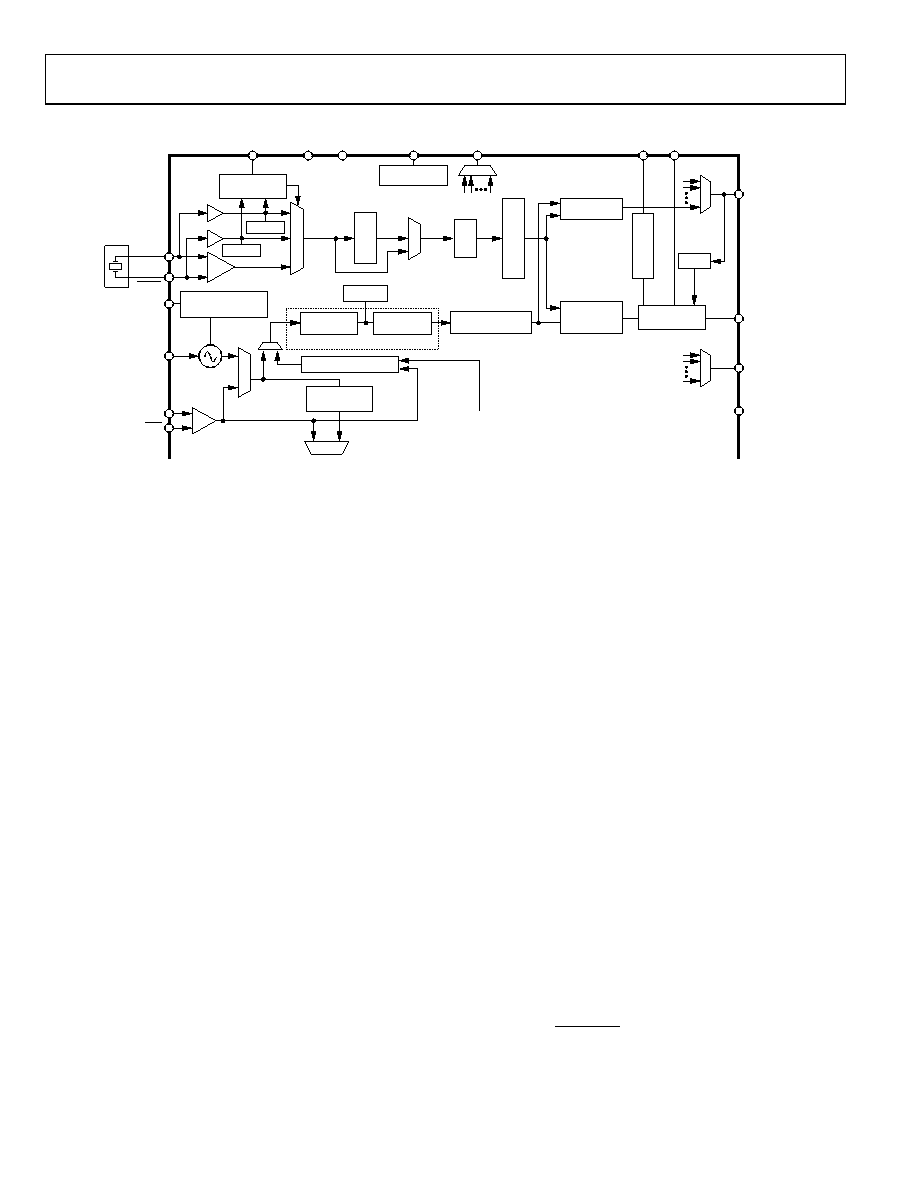
Figure 38. PLL Functional Block Diagram
The AD9520 includes an on-chip PLL with an on-chip VCO.
The PLL blocks can be used either with the on-chip VCO to
create a complete phase-locked loop or with an external VCO
or VCXO. The PLL requires an external loop filter, which
usually consists of a small number of capacitors and resistors.
The configuration and components of the loop filter help to
establish the loop bandwidth and stability of the operating PLL.
The AD9520 PLL is useful for generating clock frequencies
from a supplied reference frequency. This includes conversion
of reference frequencies to much higher frequencies for subsequent
division and distribution. In addition, the PLL can be used to
clean up jitter and phase noise on a noisy reference. The exact
choice of PLL parameters and loop dynamics is application
specific. The flexibility and depth of the AD9520 PLL allow the
part to be tailored to function in many different applications
and signal environments.
Configuration of the PLL
The AD9520 allows flexible configuration of the PLL, which
accommodates various reference frequencies, PFD comparison
frequencies, VCO frequencies, internal or external VCO/VCXO,
and loop dynamics. This is accomplished by the various settings
for the R divider, N divider, PFD polarity (applicable only to the
external VCO/VCXO), antibacklash pulse width, charge pump
current, selection of internal VCO or external VCO/ VCXO, and
the loop bandwidth. These are managed through programmable
register settings (see Table 50 and Table 54) and by the design of
the external loop filter. Successful PLL operation and satisfactory
PLL loop performance are highly dependent upon proper
configuration of the PLL settings, and the design of the external
loop filter is crucial to the proper operation of the PLL.
ADIsimCLK is a free program that can help with the design
and exploration of the capabilities and features of the AD9520,
including the design of the PLL loop filter.
Phase Frequency Detector (PFD)
The PFD takes inputs from the R divider and the N divider and
produces an output proportional to the phase and frequency
difference between them. The PFD includes a programmable
delay element that controls the width of the antibacklash pulse.
This pulse ensures that there is no dead zone in the PFD transfer
function and minimizes phase noise and reference spurs. The
antibacklash pulse width is set by Register 0x017[1:0].
An important limit to keep in mind is the maximum frequency
allowed into the PFD. The maximum input frequency into the
PFD is a function of the antibacklash pulse setting, as specified
in the phase/frequency detector (PFD) parameter in Table 2.
Charge Pump (CP)
The charge pump is controlled by the PFD. The PFD monitors
the phase and frequency relationship between its two inputs and
tells the CP to pump up or pump down to charge or discharge the
integrating node (part of the loop filter). The integrated and
filtered CP current is transformed into a voltage that drives the
tuning node of the internal VCO through the LF pin (or the tuning
pin of an external VCO) to move the VCO frequency up or down.
The CP can be set (Register 0x010[3:2]) for high impedance
(allows holdover operation), for normal operation (attempts to
lock the PLL loop), or for pump up or pump down (test modes).
The CP current is programmable in eight steps from (nominally)
0.6 mA to 4.8 mA. The CP current LSB is set by the CPRSET
resistor, which is nominally 5.1 k. The exact value of the CP
current can be calculated with the following equation:
ICP (A) =
)
(
06
.
3
RSET
CP
相关PDF资料 |
PDF描述 |
|---|---|
| AD9520-1BCPZ | IC CLOCK GEN 2.5GHZ VCO 64LFCSP |
| AD9520-2BCPZ | IC CLOCK GEN 2.2GHZ VCO 64LFCSP |
| AD9520-3BCPZ-REEL7 | IC CLOCK GEN 2GHZ VCO 64LFCSP |
| AD9520-4BCPZ-REEL7 | IC CLOCK GEN 1.6GHZ VCO 64LFCSP |
| AD9520-5BCPZ-REEL7 | IC CLOCK GEN EXT VCO 64LFCSP |
相关代理商/技术参数 |
参数描述 |
|---|---|
| AD9520-1 | 制造商:AD 制造商全称:Analog Devices 功能描述:12 LVPECL/24 CMOS Output Clock Generator with Integrated 2.5 GHz VCO |
| AD9520-1/PCBZ | 功能描述:BOARD EVAL FOR AD9520-1 RoHS:是 类别:编程器,开发系统 >> 评估演示板和套件 系列:- 标准包装:1 系列:PSoC® 主要目的:电源管理,热管理 嵌入式:- 已用 IC / 零件:- 主要属性:- 次要属性:- 已供物品:板,CD,电源 |
| AD9520-1BCPZ | 功能描述:IC CLOCK GEN 2.5GHZ VCO 64LFCSP RoHS:是 类别:集成电路 (IC) >> 时钟/计时 - 时钟发生器,PLL,频率合成器 系列:- 标准包装:2,000 系列:- 类型:PLL 时钟发生器 PLL:带旁路 输入:LVCMOS,LVPECL 输出:LVCMOS 电路数:1 比率 - 输入:输出:2:11 差分 - 输入:输出:是/无 频率 - 最大:240MHz 除法器/乘法器:是/无 电源电压:3.135 V ~ 3.465 V 工作温度:0°C ~ 70°C 安装类型:表面贴装 封装/外壳:32-LQFP 供应商设备封装:32-TQFP(7x7) 包装:带卷 (TR) |
| AD9520-1BCPZ-REEL7 | 功能描述:IC CLOCK GEN 2.5GHZ VCO 64LFCSP RoHS:是 类别:集成电路 (IC) >> 时钟/计时 - 时钟发生器,PLL,频率合成器 系列:- 标准包装:2,000 系列:- 类型:PLL 时钟发生器 PLL:带旁路 输入:LVCMOS,LVPECL 输出:LVCMOS 电路数:1 比率 - 输入:输出:2:11 差分 - 输入:输出:是/无 频率 - 最大:240MHz 除法器/乘法器:是/无 电源电压:3.135 V ~ 3.465 V 工作温度:0°C ~ 70°C 安装类型:表面贴装 封装/外壳:32-LQFP 供应商设备封装:32-TQFP(7x7) 包装:带卷 (TR) |
| AD9520-2 | 制造商:AD 制造商全称:Analog Devices 功能描述:12 LVPECL/24 CMOS Output Clock Generator with Integrated 2.2 GHz VCO |
发布紧急采购,3分钟左右您将得到回复。