- 您现在的位置:买卖IC网 > PDF目录1987 > AD9520-0BCPZ-REEL7 (Analog Devices Inc)IC CLOCK GEN 2.8GHZ VCO 64LFCSP PDF资料下载
参数资料
| 型号: | AD9520-0BCPZ-REEL7 |
| 厂商: | Analog Devices Inc |
| 文件页数: | 42/80页 |
| 文件大小: | 0K |
| 描述: | IC CLOCK GEN 2.8GHZ VCO 64LFCSP |
| 设计资源: | Synchronizing Multiple AD9910 1 GSPS Direct Digital Synthesizers (CN0121) Phase Coherent FSK Modulator (CN0186) |
| 标准包装: | 750 |
| 类型: | 时钟发生器,扇出配送 |
| PLL: | 是 |
| 输入: | CMOS,LVDS,LVPECL |
| 输出: | CMOS,LVPECL |
| 电路数: | 1 |
| 比率 - 输入:输出: | 2:12,2:24 |
| 差分 - 输入:输出: | 是/是 |
| 频率 - 最大: | 2.95GHz |
| 除法器/乘法器: | 是/无 |
| 电源电压: | 3.135 V ~ 3.465 V |
| 工作温度: | -40°C ~ 85°C |
| 安装类型: | 表面贴装 |
| 封装/外壳: | 64-VFQFN 裸露焊盘,CSP |
| 供应商设备封装: | 64-LFCSP-VQ(9x9) |
| 包装: | 带卷 (TR) |
第1页第2页第3页第4页第5页第6页第7页第8页第9页第10页第11页第12页第13页第14页第15页第16页第17页第18页第19页第20页第21页第22页第23页第24页第25页第26页第27页第28页第29页第30页第31页第32页第33页第34页第35页第36页第37页第38页第39页第40页第41页当前第42页第43页第44页第45页第46页第47页第48页第49页第50页第51页第52页第53页第54页第55页第56页第57页第58页第59页第60页第61页第62页第63页第64页第65页第66页第67页第68页第69页第70页第71页第72页第73页第74页第75页第76页第77页第78页第79页第80页
Data Sheet
AD9520-0
Rev. A | Page 47 of 80
Note that the value stored in the register equals the number of
cycles minus one. For example, Register 0x190[7:4] = 0001b
equals two low cycles (M = 2) for Divider 0.
Let
Δt = delay (in seconds).
Δc = delay (in cycles of clock signal at input to DX).
TX = period of the clock signal at the input of the divider, DX
(in seconds).
Φ =
16 × SH[4] + 8 × PO[3] + 4 × PO[2] + 2 × PO[1] + 1 × PO[0].
The channel divide-by is set as N = high cycles and M = low cycles.
Case 1
For Φ ≤ 15,
Δt = Φ × TX
Δc = Δt/TX = Φ
Case 2
For Φ ≥ 16,
Δt = (Φ 16 + M + 1) × TX
Δc = Δt/TX
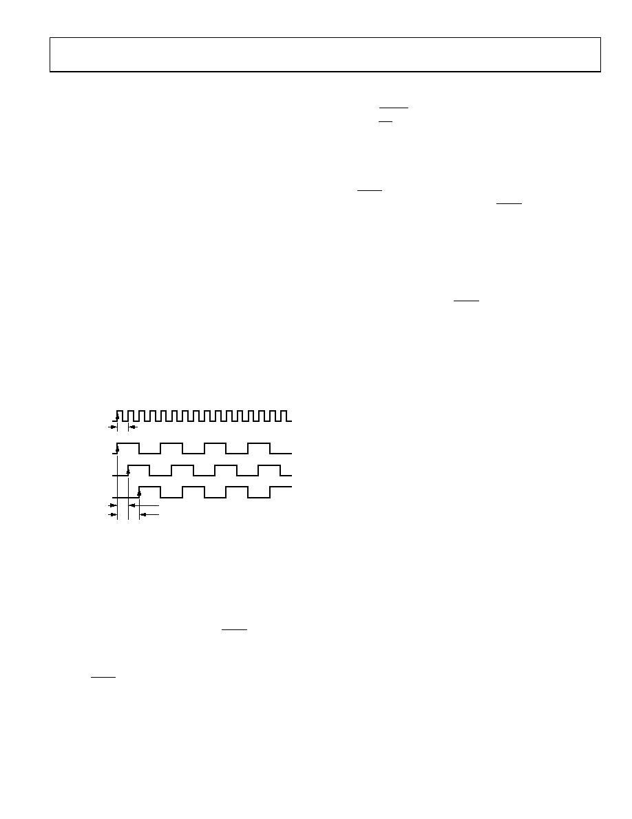
By giving each divider a different phase offset, output-to-output
delays can be set in increments of the channel divider input
clock cycle. Figure 51 shows the results of setting such a coarse
offset between outputs.
0
1
2
3
4
5
6
7
8
9
10 11 12 13 14 15
Tx
DIVIDER 0
DIVIDER 1
DIVIDER 2
CHANNEL
DIVIDER INPUT
SH = 0
PO = 0
SH = 0
PO = 1
SH = 0
PO = 2
1 × Tx
2 × Tx
CHANNEL DIVIDER OUTPUTS
DIV = 4, DUTY = 50%
07213-
071
Figure 51. Effect of Coarse Phase Offset (or Delay)
Synchronizing the Outputs—SYNC Function
The AD9520 clock outputs can be synchronized to each other.
Outputs can be individually excluded from synchronization.
Synchronization consists of setting the nonexcluded outputs to a
preset set of static conditions. These conditions include the divider
ratio and phase offsets for a given channel divider. This allows
the user to specify different divide ratios and phase offsets for each
of the four channel dividers. Releasing the SYNC pin allows the
outputs to continue clocking with the preset conditions applied.
Synchronization of the outputs is executed in the following ways:
The SYNC pin is forced low and then released (manual sync).
By setting and then resetting any one of the following three
bits: the soft SYNC bit (Register 0x230[0]), the soft reset bit
(Register 0x000[5] [mirrored]), and the power-down
distribution reference bit (Register 0x230[1]).
Synchronization of the outputs can be executed as part of
the chip power-up sequence.
The RESET pin is forced low and then released (chip reset).
The PD pin is forced low, then released (chip power-down).
When a VCO calibration is completed, an internal SYNC
signal is automatically asserted at the beginning and
released upon the completion of a VCO calibration.
The most common way to execute the SYNC function is to use
the SYNC pin to perform a manual synchronization of the outputs.
This requires a low going signal on the SYNC pin, which is held
low and then released when synchronization is desired.
The timing of the SYNC operation is shown in Figure 52 (using
the VCO divider) and in Figure 53 (the VCO divider is not used).
There is an uncertainty of up to one cycle of the clock at the input
to the channel divider due to the asynchronous nature of the
SYNC signal with respect to the clock edges inside the AD9520.
The pipeline delay from the SYNC rising edge to the beginning
of the synchronized output clocking is between 14 cycles and
15 cycles of clock at the channel divider input, plus either one
cycle of the VCO divider input (see Figure 52), or one cycle of
the channel divider input (see Figure 53), depending on whether
the VCO divider is used. Cycles are counted from the rising
edge of the signal. In addition, there is an additional 1.2 ns (typical)
delay from the SYNC signal to the internal synchronization logic,
as well as the propagation delay of the output driver. The driver
propagation delay is approximately 100 ps for the LVPECL
driver and approximately 1.5 ns for the CMOS driver.
Another common way to execute the SYNC function is by
setting and resetting the soft SYNC bit at Register 0x230[0]. Both
setting and resetting of the soft SYNC bit require an update all
registers (Register 0x232[0] = 1b) operation to take effect.
A SYNC operation brings all outputs that have not been excluded
(by the ignore SYNC bit) to a preset condition before allowing
the outputs to begin clocking in synchronicity. The preset condition
takes into account the settings in each of the channel’s start high
bit and its phase offset. These settings govern both the static state
of each output when the SYNC operation is happening and the
state and relative phase of the outputs when they begin clocking
again upon completion of the SYNC operation. Between outputs
and after synchronization, this allows for the setting of phase offsets.
The AD9520 differential LVPECL outputs are four groups of
three, sharing a channel divider per triplet. In the case of CMOS,
each LVPECL differential pair can be configured as two single-
ended CMOS outputs. The synchronization conditions apply to
all of the drivers that belong to that channel divider.
Each channel (a divider and its outputs) can be excluded from
any SYNC operation by setting the ignore SYNC bit of the channel.
Channels that are set to ignore SYNC (excluded channels) do not
set their outputs static during a SYNC operation, and their outputs
are not synchronized with those of the included channels.
相关PDF资料 |
PDF描述 |
|---|---|
| AD9520-1BCPZ | IC CLOCK GEN 2.5GHZ VCO 64LFCSP |
| AD9520-2BCPZ | IC CLOCK GEN 2.2GHZ VCO 64LFCSP |
| AD9520-3BCPZ-REEL7 | IC CLOCK GEN 2GHZ VCO 64LFCSP |
| AD9520-4BCPZ-REEL7 | IC CLOCK GEN 1.6GHZ VCO 64LFCSP |
| AD9520-5BCPZ-REEL7 | IC CLOCK GEN EXT VCO 64LFCSP |
相关代理商/技术参数 |
参数描述 |
|---|---|
| AD9520-1 | 制造商:AD 制造商全称:Analog Devices 功能描述:12 LVPECL/24 CMOS Output Clock Generator with Integrated 2.5 GHz VCO |
| AD9520-1/PCBZ | 功能描述:BOARD EVAL FOR AD9520-1 RoHS:是 类别:编程器,开发系统 >> 评估演示板和套件 系列:- 标准包装:1 系列:PSoC® 主要目的:电源管理,热管理 嵌入式:- 已用 IC / 零件:- 主要属性:- 次要属性:- 已供物品:板,CD,电源 |
| AD9520-1BCPZ | 功能描述:IC CLOCK GEN 2.5GHZ VCO 64LFCSP RoHS:是 类别:集成电路 (IC) >> 时钟/计时 - 时钟发生器,PLL,频率合成器 系列:- 标准包装:2,000 系列:- 类型:PLL 时钟发生器 PLL:带旁路 输入:LVCMOS,LVPECL 输出:LVCMOS 电路数:1 比率 - 输入:输出:2:11 差分 - 输入:输出:是/无 频率 - 最大:240MHz 除法器/乘法器:是/无 电源电压:3.135 V ~ 3.465 V 工作温度:0°C ~ 70°C 安装类型:表面贴装 封装/外壳:32-LQFP 供应商设备封装:32-TQFP(7x7) 包装:带卷 (TR) |
| AD9520-1BCPZ-REEL7 | 功能描述:IC CLOCK GEN 2.5GHZ VCO 64LFCSP RoHS:是 类别:集成电路 (IC) >> 时钟/计时 - 时钟发生器,PLL,频率合成器 系列:- 标准包装:2,000 系列:- 类型:PLL 时钟发生器 PLL:带旁路 输入:LVCMOS,LVPECL 输出:LVCMOS 电路数:1 比率 - 输入:输出:2:11 差分 - 输入:输出:是/无 频率 - 最大:240MHz 除法器/乘法器:是/无 电源电压:3.135 V ~ 3.465 V 工作温度:0°C ~ 70°C 安装类型:表面贴装 封装/外壳:32-LQFP 供应商设备封装:32-TQFP(7x7) 包装:带卷 (TR) |
| AD9520-2 | 制造商:AD 制造商全称:Analog Devices 功能描述:12 LVPECL/24 CMOS Output Clock Generator with Integrated 2.2 GHz VCO |
发布紧急采购,3分钟左右您将得到回复。