- 您现在的位置:买卖IC网 > PDF目录1987 > AD9520-0BCPZ-REEL7 (Analog Devices Inc)IC CLOCK GEN 2.8GHZ VCO 64LFCSP PDF资料下载
参数资料
| 型号: | AD9520-0BCPZ-REEL7 |
| 厂商: | Analog Devices Inc |
| 文件页数: | 72/80页 |
| 文件大小: | 0K |
| 描述: | IC CLOCK GEN 2.8GHZ VCO 64LFCSP |
| 设计资源: | Synchronizing Multiple AD9910 1 GSPS Direct Digital Synthesizers (CN0121) Phase Coherent FSK Modulator (CN0186) |
| 标准包装: | 750 |
| 类型: | 时钟发生器,扇出配送 |
| PLL: | 是 |
| 输入: | CMOS,LVDS,LVPECL |
| 输出: | CMOS,LVPECL |
| 电路数: | 1 |
| 比率 - 输入:输出: | 2:12,2:24 |
| 差分 - 输入:输出: | 是/是 |
| 频率 - 最大: | 2.95GHz |
| 除法器/乘法器: | 是/无 |
| 电源电压: | 3.135 V ~ 3.465 V |
| 工作温度: | -40°C ~ 85°C |
| 安装类型: | 表面贴装 |
| 封装/外壳: | 64-VFQFN 裸露焊盘,CSP |
| 供应商设备封装: | 64-LFCSP-VQ(9x9) |
| 包装: | 带卷 (TR) |
第1页第2页第3页第4页第5页第6页第7页第8页第9页第10页第11页第12页第13页第14页第15页第16页第17页第18页第19页第20页第21页第22页第23页第24页第25页第26页第27页第28页第29页第30页第31页第32页第33页第34页第35页第36页第37页第38页第39页第40页第41页第42页第43页第44页第45页第46页第47页第48页第49页第50页第51页第52页第53页第54页第55页第56页第57页第58页第59页第60页第61页第62页第63页第64页第65页第66页第67页第68页第69页第70页第71页当前第72页第73页第74页第75页第76页第77页第78页第79页第80页
AD9520-0
Data Sheet
Rev. A | Page 74 of 80
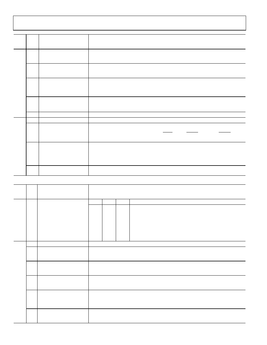
Reg.
Addr.
(Hex) Bits
Name
Description
0x19A 7
Divider 3 bypass
Bypasses and powers down the divider; routes input to divider output.
0: uses divider (default).
1: bypasses divider.
6
Divider 3 ignore SYNC
Ignores SYNC.
0: obeys chip-level SYNC signal (default).
1: ignores chip-level SYNC signal.
5
Divider 3 force high
Forces divider output to a specific state. This requires that ignore SYNC also be set. Note that
this bit has no effect if the channel divider is bypassed, but the driver polarity can still be reversed.
0: divider output is forced to low (default).
1: divider output is forced to the setting stored in Bit 4 of this register.
4
Divider 3 start high
Selects clock output to start high or start low.
0: starts low (default).
1: starts high.
[3:0]
Divider 3 phase offset
Phase offset (default: 0x0).
0x19B [7:3]
Unused
Unused.
2
Channel 3 power-down
Channel 3 powers down.
0: normal operation (default).
1: powered down. (Setting this bit puts OUT9/OUT9, OUT10/OUT10, and OUT11/OUT11 into
safe power-down mode.)
1
Channel 3 direct to output
Connects OUT9, OUT10, and OUT11 to Divider 3 or directly to VCO or CLK.
0: OUT9, OUT10, and OUT11 are connected to Divider 3 (default).
1: If Register 0x1E1[1:0] = 10b, the VCO is routed directly to OUT9, OUT10, and OUT11.
If Register 0x1E1[1:0] = 00b, the CLK is routed directly to OUT9, OUT10, and OUT11.
If Register 0x1E1[1:0] = 01b, there is no effect.
0
Disable Divider 3 DCC
Duty-cycle correction function.
0: enables duty-cycle correction (default); 1: disables duty-cycle correction.
Table 57. VCO Divider and CLK Input
Reg.
Addr.
(Hex) Bits Name
Description
0x1E0 [2:0] VCO divider
Bit 2
Bit 1
Bit 0
Divide
0
1
0
1
0
1
0
1
0
1
0
1
0
1
2 (default)
3
4
5
6
Output static
1 (bypass)
Output static
0x1E1 [7:5] Unused
Unused.
4
Power down clock input section Powers down the clock input section (including CLK buffer, VCO divider, and CLK tree).
0: normal operation (default).
1: power-down.
3
Power down VCO clock
interface
Powers down the interface block between VCO and clock distribution.
0: normal operation (default).
1: power-down.
2
Power down VCO and CLK
Powers down both the VCO and the CLK input.
0: normal operation (default).
1: power-down.
1
Select VCO or CLK
Selects either the VCO or the CLK as the input to VCO divider.
0: selects external CLK as input to VCO divider (default).
1: selects VCO as input to VCO divider; VCO divider cannot be bypassed when this bit is set.
This bit must be set to use the PLL with the internal VCO.
0
Bypass VCO divider
Bypasses or uses the VCO divider.
0: uses VCO divider (default).
1: bypasses VCO divider; VCO cannot be selected as input when this bit is set.
相关PDF资料 |
PDF描述 |
|---|---|
| AD9520-1BCPZ | IC CLOCK GEN 2.5GHZ VCO 64LFCSP |
| AD9520-2BCPZ | IC CLOCK GEN 2.2GHZ VCO 64LFCSP |
| AD9520-3BCPZ-REEL7 | IC CLOCK GEN 2GHZ VCO 64LFCSP |
| AD9520-4BCPZ-REEL7 | IC CLOCK GEN 1.6GHZ VCO 64LFCSP |
| AD9520-5BCPZ-REEL7 | IC CLOCK GEN EXT VCO 64LFCSP |
相关代理商/技术参数 |
参数描述 |
|---|---|
| AD9520-1 | 制造商:AD 制造商全称:Analog Devices 功能描述:12 LVPECL/24 CMOS Output Clock Generator with Integrated 2.5 GHz VCO |
| AD9520-1/PCBZ | 功能描述:BOARD EVAL FOR AD9520-1 RoHS:是 类别:编程器,开发系统 >> 评估演示板和套件 系列:- 标准包装:1 系列:PSoC® 主要目的:电源管理,热管理 嵌入式:- 已用 IC / 零件:- 主要属性:- 次要属性:- 已供物品:板,CD,电源 |
| AD9520-1BCPZ | 功能描述:IC CLOCK GEN 2.5GHZ VCO 64LFCSP RoHS:是 类别:集成电路 (IC) >> 时钟/计时 - 时钟发生器,PLL,频率合成器 系列:- 标准包装:2,000 系列:- 类型:PLL 时钟发生器 PLL:带旁路 输入:LVCMOS,LVPECL 输出:LVCMOS 电路数:1 比率 - 输入:输出:2:11 差分 - 输入:输出:是/无 频率 - 最大:240MHz 除法器/乘法器:是/无 电源电压:3.135 V ~ 3.465 V 工作温度:0°C ~ 70°C 安装类型:表面贴装 封装/外壳:32-LQFP 供应商设备封装:32-TQFP(7x7) 包装:带卷 (TR) |
| AD9520-1BCPZ-REEL7 | 功能描述:IC CLOCK GEN 2.5GHZ VCO 64LFCSP RoHS:是 类别:集成电路 (IC) >> 时钟/计时 - 时钟发生器,PLL,频率合成器 系列:- 标准包装:2,000 系列:- 类型:PLL 时钟发生器 PLL:带旁路 输入:LVCMOS,LVPECL 输出:LVCMOS 电路数:1 比率 - 输入:输出:2:11 差分 - 输入:输出:是/无 频率 - 最大:240MHz 除法器/乘法器:是/无 电源电压:3.135 V ~ 3.465 V 工作温度:0°C ~ 70°C 安装类型:表面贴装 封装/外壳:32-LQFP 供应商设备封装:32-TQFP(7x7) 包装:带卷 (TR) |
| AD9520-2 | 制造商:AD 制造商全称:Analog Devices 功能描述:12 LVPECL/24 CMOS Output Clock Generator with Integrated 2.2 GHz VCO |
发布紧急采购,3分钟左右您将得到回复。