- 您现在的位置:买卖IC网 > PDF目录1987 > AD9520-0BCPZ-REEL7 (Analog Devices Inc)IC CLOCK GEN 2.8GHZ VCO 64LFCSP PDF资料下载
参数资料
| 型号: | AD9520-0BCPZ-REEL7 |
| 厂商: | Analog Devices Inc |
| 文件页数: | 68/80页 |
| 文件大小: | 0K |
| 描述: | IC CLOCK GEN 2.8GHZ VCO 64LFCSP |
| 设计资源: | Synchronizing Multiple AD9910 1 GSPS Direct Digital Synthesizers (CN0121) Phase Coherent FSK Modulator (CN0186) |
| 标准包装: | 750 |
| 类型: | 时钟发生器,扇出配送 |
| PLL: | 是 |
| 输入: | CMOS,LVDS,LVPECL |
| 输出: | CMOS,LVPECL |
| 电路数: | 1 |
| 比率 - 输入:输出: | 2:12,2:24 |
| 差分 - 输入:输出: | 是/是 |
| 频率 - 最大: | 2.95GHz |
| 除法器/乘法器: | 是/无 |
| 电源电压: | 3.135 V ~ 3.465 V |
| 工作温度: | -40°C ~ 85°C |
| 安装类型: | 表面贴装 |
| 封装/外壳: | 64-VFQFN 裸露焊盘,CSP |
| 供应商设备封装: | 64-LFCSP-VQ(9x9) |
| 包装: | 带卷 (TR) |
第1页第2页第3页第4页第5页第6页第7页第8页第9页第10页第11页第12页第13页第14页第15页第16页第17页第18页第19页第20页第21页第22页第23页第24页第25页第26页第27页第28页第29页第30页第31页第32页第33页第34页第35页第36页第37页第38页第39页第40页第41页第42页第43页第44页第45页第46页第47页第48页第49页第50页第51页第52页第53页第54页第55页第56页第57页第58页第59页第60页第61页第62页第63页第64页第65页第66页第67页当前第68页第69页第70页第71页第72页第73页第74页第75页第76页第77页第78页第79页第80页
AD9520-0
Data Sheet
Rev. A | Page 70 of 80
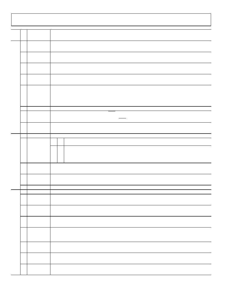
Reg.
Addr.
(Hex) Bits Name
Description
0x01D 7
Enable
STATUS_EEPROM
at STATUS pin
Enables the STATUS_EEPROM signal at the STATUS pin.
0: the STATUS pin is controlled by the Register 0x017[7:2] selection.
1: selects the STATUS_EEPROM signal at the STATUS pin. This bit overrides the Register 0x017[7:2] selection (default).
6
Enable XTAL OSC Enables the maintaining amplifier needed by a crystal oscillator at the PLL reference input.
0: crystal oscillator maintaining amplifier disabled (default).
1: crystal oscillator maintaining amplifier enabled.
5
Enable clock
doubler
Enables PLL reference input clock doubler.
0: doubler disabled (default).
1: doubler enabled.
4
Disable PLL
status register
Disables the PLL status register readback.
0: PLL status register enabled (default).
1: PLL status register disabled. If this bit is set, Register 0x01F is not automatically updated.
3
Enable LD pin
comparator
Enables the LD pin voltage comparator. Used with the LD pin current source lock detect mode. When the AD9520 is in internal
(automatic) holdover mode, this bit enables the use of the voltage on the LD pin to determine if the PLL was previously in
a locked state (see Figure 47). Otherwise, this can be used with the REFMON and STATUS pins to monitor the voltage on the LD pin.
0: disables LD pin comparator and ignores the LD pin voltage; the automatic/internal holdover controller treats this pin as true
(high, default).
1: enables the LD pin comparator (uses the LD pin voltage to determine if the PLL was previously locked).
2
Unused
Unused.
1
Enable external
holdover
Enables the external hold control through the SYNC pin. (This bit disables the internal holdover mode.)
0: automatic holdover mode; holdover controlled by the automatic holdover circuit (default).
1: external holdover mode; holdover controlled by the SYNC pin.
0
Enable holdover Enables the internally controlled holdover function.
0: holdover disabled (default).
1: holdover enabled.
0x01E [7:5] Unused
Unused.
[4:3] External zero
delay feedback
channel divider
select
Bit
4
Bit
3
Selection of Channel Divider for Use in the External Zero-Delay Path
0
Selects Channel Divider 0 (default).
0
1
Selects Channel Divider 1.
1
0
Selects Channel Divider 2.
1
Selects Channel Divider 3.
2
Enable external
zero delay
Selects which zero delay mode to use.
0: enables internal zero delay mode if Register 0x01E[1] = 1 (default).
1: enables external zero delay mode if Register 0x01E[1] = 1.
1
Enable
zero delay
Enables zero delay function.
0: disables zero delay function (default).
1: enables zero delay function.
0
Unused
Unused.
0x01F 7
Unused
Unused.
6
VCO calibration
finished
(read only)
Readback register. Indicates the status of the VCO calibration.
0: VCO calibration not finished.
1: VCO calibration finished.
5
Holdover active
(read only)
Readback register. Indicates if the part is in the holdover state (see Figure 47). Note that this is not the same as holdover enabled.
0: not in holdover state.
1: holdover state active.
4
REF2 selected
(read only)
Readback register. Indicates which PLL reference is selected as the input to the PLL.
0: REF1 selected (or differential reference if in differential mode).
1: REF2 selected.
3
VCO frequency >
threshold
(read only)
Readback register. Indicates if the VCO frequency is greater than the threshold (see Table 17: REF1, REF2, and VCO frequency
status monitor parameter).
0: VCO frequency is less than the threshold.
1: VCO frequency is greater than the threshold.
2
REF2 frequency >
threshold
(read only)
Readback register. Indicates if the frequency of the signal at REF2 is greater than the threshold frequency set by Register 0x01A[6].
0: REF2 frequency is less than the threshold frequency.
1: REF2 frequency is greater than the threshold frequency.
1
REF1 frequency >
threshold
(read only)
Readback register. Indicates if the frequency of the signal at REF1 is greater than the threshold frequency set by Register 0x01A[6].
0: REF1 frequency is less than the threshold frequency.
1: REF1 frequency is greater than the threshold frequency.
0
Digital lock
detect
(read only)
Readback register. Digital lock detect.
0: PLL is not locked.
1: PLL is locked.
相关PDF资料 |
PDF描述 |
|---|---|
| AD9520-1BCPZ | IC CLOCK GEN 2.5GHZ VCO 64LFCSP |
| AD9520-2BCPZ | IC CLOCK GEN 2.2GHZ VCO 64LFCSP |
| AD9520-3BCPZ-REEL7 | IC CLOCK GEN 2GHZ VCO 64LFCSP |
| AD9520-4BCPZ-REEL7 | IC CLOCK GEN 1.6GHZ VCO 64LFCSP |
| AD9520-5BCPZ-REEL7 | IC CLOCK GEN EXT VCO 64LFCSP |
相关代理商/技术参数 |
参数描述 |
|---|---|
| AD9520-1 | 制造商:AD 制造商全称:Analog Devices 功能描述:12 LVPECL/24 CMOS Output Clock Generator with Integrated 2.5 GHz VCO |
| AD9520-1/PCBZ | 功能描述:BOARD EVAL FOR AD9520-1 RoHS:是 类别:编程器,开发系统 >> 评估演示板和套件 系列:- 标准包装:1 系列:PSoC® 主要目的:电源管理,热管理 嵌入式:- 已用 IC / 零件:- 主要属性:- 次要属性:- 已供物品:板,CD,电源 |
| AD9520-1BCPZ | 功能描述:IC CLOCK GEN 2.5GHZ VCO 64LFCSP RoHS:是 类别:集成电路 (IC) >> 时钟/计时 - 时钟发生器,PLL,频率合成器 系列:- 标准包装:2,000 系列:- 类型:PLL 时钟发生器 PLL:带旁路 输入:LVCMOS,LVPECL 输出:LVCMOS 电路数:1 比率 - 输入:输出:2:11 差分 - 输入:输出:是/无 频率 - 最大:240MHz 除法器/乘法器:是/无 电源电压:3.135 V ~ 3.465 V 工作温度:0°C ~ 70°C 安装类型:表面贴装 封装/外壳:32-LQFP 供应商设备封装:32-TQFP(7x7) 包装:带卷 (TR) |
| AD9520-1BCPZ-REEL7 | 功能描述:IC CLOCK GEN 2.5GHZ VCO 64LFCSP RoHS:是 类别:集成电路 (IC) >> 时钟/计时 - 时钟发生器,PLL,频率合成器 系列:- 标准包装:2,000 系列:- 类型:PLL 时钟发生器 PLL:带旁路 输入:LVCMOS,LVPECL 输出:LVCMOS 电路数:1 比率 - 输入:输出:2:11 差分 - 输入:输出:是/无 频率 - 最大:240MHz 除法器/乘法器:是/无 电源电压:3.135 V ~ 3.465 V 工作温度:0°C ~ 70°C 安装类型:表面贴装 封装/外壳:32-LQFP 供应商设备封装:32-TQFP(7x7) 包装:带卷 (TR) |
| AD9520-2 | 制造商:AD 制造商全称:Analog Devices 功能描述:12 LVPECL/24 CMOS Output Clock Generator with Integrated 2.2 GHz VCO |
发布紧急采购,3分钟左右您将得到回复。