- 您现在的位置:买卖IC网 > PDF目录1987 > AD9520-0BCPZ-REEL7 (Analog Devices Inc)IC CLOCK GEN 2.8GHZ VCO 64LFCSP PDF资料下载
参数资料
| 型号: | AD9520-0BCPZ-REEL7 |
| 厂商: | Analog Devices Inc |
| 文件页数: | 21/80页 |
| 文件大小: | 0K |
| 描述: | IC CLOCK GEN 2.8GHZ VCO 64LFCSP |
| 设计资源: | Synchronizing Multiple AD9910 1 GSPS Direct Digital Synthesizers (CN0121) Phase Coherent FSK Modulator (CN0186) |
| 标准包装: | 750 |
| 类型: | 时钟发生器,扇出配送 |
| PLL: | 是 |
| 输入: | CMOS,LVDS,LVPECL |
| 输出: | CMOS,LVPECL |
| 电路数: | 1 |
| 比率 - 输入:输出: | 2:12,2:24 |
| 差分 - 输入:输出: | 是/是 |
| 频率 - 最大: | 2.95GHz |
| 除法器/乘法器: | 是/无 |
| 电源电压: | 3.135 V ~ 3.465 V |
| 工作温度: | -40°C ~ 85°C |
| 安装类型: | 表面贴装 |
| 封装/外壳: | 64-VFQFN 裸露焊盘,CSP |
| 供应商设备封装: | 64-LFCSP-VQ(9x9) |
| 包装: | 带卷 (TR) |
第1页第2页第3页第4页第5页第6页第7页第8页第9页第10页第11页第12页第13页第14页第15页第16页第17页第18页第19页第20页当前第21页第22页第23页第24页第25页第26页第27页第28页第29页第30页第31页第32页第33页第34页第35页第36页第37页第38页第39页第40页第41页第42页第43页第44页第45页第46页第47页第48页第49页第50页第51页第52页第53页第54页第55页第56页第57页第58页第59页第60页第61页第62页第63页第64页第65页第66页第67页第68页第69页第70页第71页第72页第73页第74页第75页第76页第77页第78页第79页第80页
AD9520-0
Data Sheet
Rev. A | Page 28 of 80
THEORY OF OPERATION
OPERATIONAL CONFIGURATIONS
The AD9520 can be configured in several ways. These
configurations must be set up by loading the control registers
(see Table 50 to Table 61). Each section or function must be
individually programmed by setting the appropriate bits in the
corresponding control register or registers. After the desired
configuration is programmed, the user can store these values in the
on-board EEPROM to allow the part to power up in the desired
configuration without user intervention.
Mode 0—Internal VCO and Clock Distribution
When the internal VCO and PLL are used, the VCO divider
must also be used, in most cases, to ensure that the frequency
presented to the channel dividers does not exceed its specified
maximum frequency (see Table 3). The exceptions to this are
the VCO direct mode and cases where the VCO frequency is
≤1600 MHz. The internal PLL uses an external loop filter to set
the loop bandwidth. The external loop filter is also crucial to
the loop stability.
When the internal VCO is used, the VCO must be calibrated
(Register 0x018[0] = 1b) to ensure optimal performance.
For internal VCO and clock distribution applications, use the
register settings shown in Table 22.
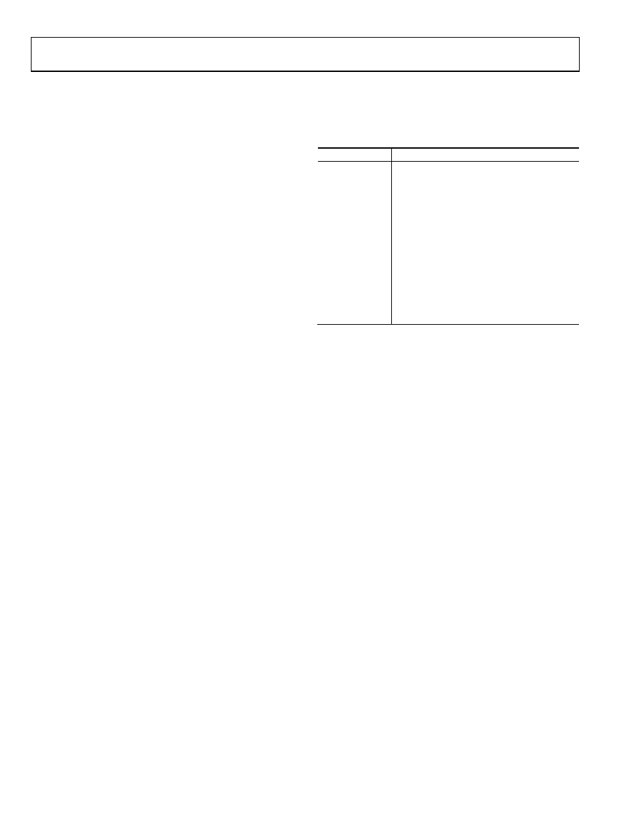
Table 22. Settings When Using Internal VCO
Register
Description
0x010[1:0] = 00b
PLL normal operation (PLL on)
0x010 to 0x01E
PLL settings; select and enable a reference
input; set R, N (P, A, B), PFD polarity, and ICP
according to the intended loop configuration
0x1E1[1] = 1b
Select VCO as the source
0x01C[2:0]
Enable reference inputs
0x1E0[2:0]
Set VCO divider
0x1E1[0] = 0b
Use the VCO divider as the source for the
distribution section
0x018[0] = 0b,
0x232[0] = 1b
Clear previous VCO calibration and issue
IO_UPDATE (not necessary the first time after
power-up, but must be done subsequently)
0x018[0] = 1b,
0x232[0] = 1b
Initiate VCO calibration, issue IO_UPDATE
相关PDF资料 |
PDF描述 |
|---|---|
| AD9520-1BCPZ | IC CLOCK GEN 2.5GHZ VCO 64LFCSP |
| AD9520-2BCPZ | IC CLOCK GEN 2.2GHZ VCO 64LFCSP |
| AD9520-3BCPZ-REEL7 | IC CLOCK GEN 2GHZ VCO 64LFCSP |
| AD9520-4BCPZ-REEL7 | IC CLOCK GEN 1.6GHZ VCO 64LFCSP |
| AD9520-5BCPZ-REEL7 | IC CLOCK GEN EXT VCO 64LFCSP |
相关代理商/技术参数 |
参数描述 |
|---|---|
| AD9520-1 | 制造商:AD 制造商全称:Analog Devices 功能描述:12 LVPECL/24 CMOS Output Clock Generator with Integrated 2.5 GHz VCO |
| AD9520-1/PCBZ | 功能描述:BOARD EVAL FOR AD9520-1 RoHS:是 类别:编程器,开发系统 >> 评估演示板和套件 系列:- 标准包装:1 系列:PSoC® 主要目的:电源管理,热管理 嵌入式:- 已用 IC / 零件:- 主要属性:- 次要属性:- 已供物品:板,CD,电源 |
| AD9520-1BCPZ | 功能描述:IC CLOCK GEN 2.5GHZ VCO 64LFCSP RoHS:是 类别:集成电路 (IC) >> 时钟/计时 - 时钟发生器,PLL,频率合成器 系列:- 标准包装:2,000 系列:- 类型:PLL 时钟发生器 PLL:带旁路 输入:LVCMOS,LVPECL 输出:LVCMOS 电路数:1 比率 - 输入:输出:2:11 差分 - 输入:输出:是/无 频率 - 最大:240MHz 除法器/乘法器:是/无 电源电压:3.135 V ~ 3.465 V 工作温度:0°C ~ 70°C 安装类型:表面贴装 封装/外壳:32-LQFP 供应商设备封装:32-TQFP(7x7) 包装:带卷 (TR) |
| AD9520-1BCPZ-REEL7 | 功能描述:IC CLOCK GEN 2.5GHZ VCO 64LFCSP RoHS:是 类别:集成电路 (IC) >> 时钟/计时 - 时钟发生器,PLL,频率合成器 系列:- 标准包装:2,000 系列:- 类型:PLL 时钟发生器 PLL:带旁路 输入:LVCMOS,LVPECL 输出:LVCMOS 电路数:1 比率 - 输入:输出:2:11 差分 - 输入:输出:是/无 频率 - 最大:240MHz 除法器/乘法器:是/无 电源电压:3.135 V ~ 3.465 V 工作温度:0°C ~ 70°C 安装类型:表面贴装 封装/外壳:32-LQFP 供应商设备封装:32-TQFP(7x7) 包装:带卷 (TR) |
| AD9520-2 | 制造商:AD 制造商全称:Analog Devices 功能描述:12 LVPECL/24 CMOS Output Clock Generator with Integrated 2.2 GHz VCO |
发布紧急采购,3分钟左右您将得到回复。