- 您现在的位置:买卖IC网 > PDF目录20639 > ADE7878ACPZ (Analog Devices Inc)IC ENERGY METERING 3PH 40LFCSP PDF资料下载
参数资料
| 型号: | ADE7878ACPZ |
| 厂商: | Analog Devices Inc |
| 文件页数: | 66/100页 |
| 文件大小: | 0K |
| 描述: | IC ENERGY METERING 3PH 40LFCSP |
| 标准包装: | 1 |
| 输入阻抗: | 400 千欧 |
| 测量误差: | 0.2% |
| 电压 - 高输入/输出: | 2.4V |
| 电压 - 低输入/输出: | 0.4V |
| 电源电压: | 2.4 V ~ 3.7 V |
| 测量仪表类型: | 3 相 |
| 工作温度: | -40°C ~ 85°C |
| 安装类型: | 表面贴装 |
| 封装/外壳: | 40-WFQFN 裸露焊盘,CSP |
| 供应商设备封装: | 40-LFCSP-WQ(6x6) |
| 包装: | 托盘 |
第1页第2页第3页第4页第5页第6页第7页第8页第9页第10页第11页第12页第13页第14页第15页第16页第17页第18页第19页第20页第21页第22页第23页第24页第25页第26页第27页第28页第29页第30页第31页第32页第33页第34页第35页第36页第37页第38页第39页第40页第41页第42页第43页第44页第45页第46页第47页第48页第49页第50页第51页第52页第53页第54页第55页第56页第57页第58页第59页第60页第61页第62页第63页第64页第65页当前第66页第67页第68页第69页第70页第71页第72页第73页第74页第75页第76页第77页第78页第79页第80页第81页第82页第83页第84页第85页第86页第87页第88页第89页第90页第91页第92页第93页第94页第95页第96页第97页第98页第99页第100页
�� �
�
�ADE7854/ADE7858/ADE7868/ADE7878�
�default� values.� The� ADE78xx� computes� the� cyclic� redundancy�
�check� (CRC)� based� on� the� IEEE802.3� standard.� The� registers�
�are� introduced� one-by-one� into� a� linear� feedback� shift� register�
�(LFSR)� based� generator� starting� with� the� least� significant� bit� (as�
�shown� in� Figure� 82).� The� 32-bit� result� is� written� in� the�
�CHECKSUM� register.� After� power-up� or� a� hardware/software�
�reset,� the� CRC� is� computed� on� the� default� values� of� the� registers�
��Data� Sheet�
�g� i� ,� i� =� 0,� 1,� 2,� …,� 31� are� the� coefficients� of� the� generating�
�polynomial� defined� by� the� IEEE802.3� standard� as� follows:�
�G� (� x� )� =� x� 32� +� x� 26� +� x� 23� +� x� 22� +� x� 16� +� x� 12� +� x� 11� +� x� 10� +� x� 8� +� x� 7� +�
�x� 5� +� x� 4� +� x� 2� +� x� +� 1� (49)�
�g� 0� =� g� 1� =� g� 2� =� g� 4� =� g� 5� =� g� 7� =� 1�
�g� 8� =� g� 10� =� g� 11� =� g� 12� =� g� 16� =� g� 22� =� g� 23� =� g� 26� =� 1� (50)�
�All� of� the� other� g� i� coefficients� are� equal� to� 0.�
�Table� 23.� Default� Values� of� CHECKSUM� and� of� Internal�
�FB� (� j� )� =� a� j� –� 1� XOR� b� 31� (� j� –� 1)�
�(51)�
�Registers� CRC�
�Default� Value� of�
�Part� No.� CHECKSUM�
�CRC� of� Internal�
�Registers�
�b� 0� (� j� )� =� FB� (� j� )� AND� g� 0�
�b� i� (j)� =� FB� (� j� )� AND� g� i� XOR� b� i� ?� 1� (� j� –� 1),� i� =� 1,� 2,� 3,� ...,� 31�
�(52)�
�(53)�
�ADE7854� 0x44C48F8� 0x391FBDDD�
�ADE7858� 0xD6744F93� 0x3E7D0FC1�
�ADE7868� 0x93D774E6� 0x23F7C7B1�
�ADE7878� 0x33666787� 0x2D32A389�
��COMPMODE,� gain,� CFMODE,� CF1DEN,� CF2DEN,� CF3DEN,�
�CONFIG,� MMODE,� ACCMODE,� LCYCMODE,� and� HSDC_CFG�
�registers,� and� the� six� 8-bit� reserved� internal� registers� form� the�
�bits� [a� 255� ,� a� 254� ,…,� a� 0� ]� used� by� LFSR.� Bit� a� 0� is� the� least� significant�
�bit� of� the� first� internal� register� to� enter� LFSR;� Bit� a� 255� is� the� most�
�significant� bit� of� the� MASK0� register,� the� last� register� to� enter�
�LFSR.� The� formulas� that� govern� LFSR� are� as� follows:�
�b� i� (0)� =� 1,� i� =� 0,� 1,� 2,� …,� 31,� the� initial� state� of� the� bits� that� form�
�the� CRC.� Bit� b� 0� is� the� least� significant� bit,� and� Bit� b� 31� is� the� most�
�significant.�
�Equation� 51,� Equation� 52,� and� Equation� 53� must� be� repeated� for�
�j� =� 1,� 2,� …,� 256.� The� value� written� into� the� CHECKSUM� register�
�contains� the� Bit� b� i� (256)� ,� i� =� 0,� 1,� …,� 31.� The� value� of� the� CRC,�
�after� the� bits� from� the� reserved� internal� register� have� passed�
�through� LFSR,� is� obtained� at� Step� j� =� 48� and� is� presented� in� the�
��Two� different� approaches� can� be� followed� in� using� the� CHECK-�
�SUM� register.� One� is� to� compute� the� CRC� based� on� the� relations�
�(47)� to� (53)� and� then� compare� the� value� against� the� CHECKSUM�
�register.� Another� is� to� periodically� read� the� CHECKSUM� register.�
�If� two� consecutive� readings� differ,� it� can� be� assumed� that� one� of�
���The� recommended� response� is� to� initiate� a� hardware/software�
�reset� that� sets� the� values� of� all� registers� to� the� default,� including�
�the� reserved� ones,� and� then� reinitialize� the� configuration� registers.�
�31� 0� 31� 0� 15� 0� 15� 0� 15� 0�
�MASK0� MASK1� COMPMODE� GAIN� CFMODE�
�7� 0� 7� 0�
�REGISTER� REGISTER�
�INTERNAL� INTERNAL�
�7� 0�
�INTERNAL�
�REGISTER�
�7� 0�
�INTERNAL�
�REGISTER�
�7� 0�
�INTERNAL�
�REGISTER�
�7� 0�
�INTERNAL�
�REGISTER�
�255�
�248�
�240�
�232�
�224�
�216�
�40�
�32�
�24�
�16�
�8�
�7�
�0�
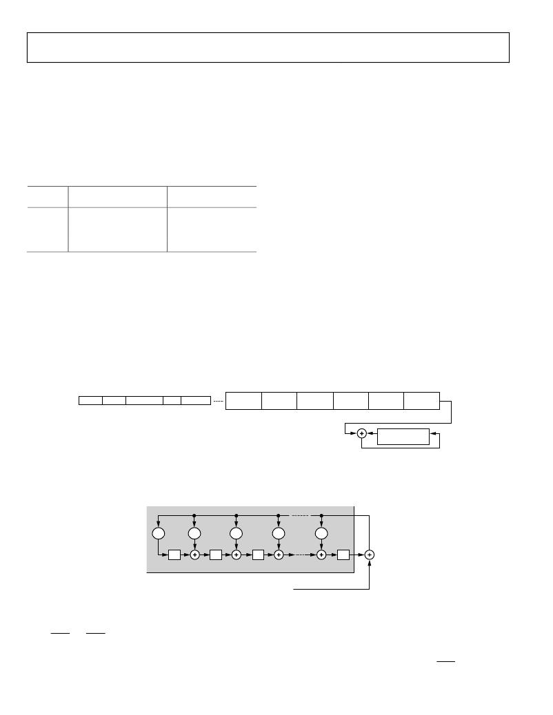
�LFSR�
�GENERATOR�
�Figure� 82.� CHECKSUM� Register� Calculation�
�g� 0�
�g� 1�
�g� 2�
�g� 3�
�g� 31�
�FB�
�b� 0�
�b� 1�
�b� 2�
�b� 31�
�LFSR�
�a� 255� ,� a� 254� ,....,� a� 2� ,� a� 1� ,� a� 0�
�Figure� 83.� LFSR� Generator� Used� in� CHECKSUM� Register� Calculation�
�INTERRUPTS�
�The� ADE7854� /� ADE7858� /� ADE7868� /� ADE7878� have� two� interrupt�
�pins,� IRQ0� and� IRQ1.� Each� of� the� pins� is� managed� by� a� 32-bit�
�interrupt� mask� register,� MASK0� and� MASK1,� respectively.� To�
�enable� an� interrupt,� a� bit� in� the� MASKx� register� must� be� set� to�
�1.� To� disable� it,� the� bit� must� be� cleared� to� 0.� Two� 32-bit� status�
�registers,� STATUS0� and� STATUS1,� are� associated� with� the� inter-�
�rupts.� When� an� interrupt� event� occurs� in� the� ADE78xx� ,� the�
�corresponding� flag� in� the� interrupt� status� register� is� set� to� a� Logic� 1�
�(see� Table� 37� and� Table� 38).� If� the� mask� bit� for� this� interrupt� in�
�the� interrupt� mask� register� is� Logic� 1,� then� the� IRQx� logic� output�
�Rev.� H� |� Page� 66� of� 100�
�相关PDF资料 |
PDF描述 |
|---|---|
| GBC06DREI-S13 | CONN EDGECARD 12POS .100 EXTEND |
| VI-J60-CX-F4 | CONVERTER MOD DC/DC 5V 75W |
| ECA10DCBT | CONN EDGECARD 20POS R/A .125 SLD |
| EL7242CSZ-T13 | IC DRIVER MOSFET DUAL HS 8-SOIC |
| ADE7169ASTZF16 | IC ENERGY METER 1PHASE 64LQFP |
相关代理商/技术参数 |
参数描述 |
|---|---|
| ADE7878ACPZ | 制造商:Analog Devices 功能描述:IC MULTIFUNCTION ENERGY METERING LFCSP40 |
| ADE7878ACPZ-RL | 功能描述:IC ENERGY METERING 3PH 40LFCSP RoHS:是 类别:集成电路 (IC) >> PMIC - 能量测量 系列:- 产品培训模块:Lead (SnPb) Finish for COTS Obsolescence Mitigation Program 标准包装:2,500 系列:* |
| ADE7878XCPZ | 制造商:Analog Devices 功能描述:POLY PHASE MULTIFUNCTION ENERGY METERING IC WITH TOTAL - Bulk |
| ADE7880 | 制造商:Analog Devices 功能描述:BOARD EVAL ENERGY METER ADE |
| ADE7880ACPZ | 功能描述:IC ENERGY METERING 3PH 40LFCSP RoHS:是 类别:集成电路 (IC) >> PMIC - 能量测量 系列:- 产品培训模块:Lead (SnPb) Finish for COTS Obsolescence Mitigation Program 标准包装:2,500 系列:* |
发布紧急采购,3分钟左右您将得到回复。