- 您现在的位置:买卖IC网 > PDF目录189449 > OR4E062BM680-DB (LATTICE SEMICONDUCTOR CORP) FPGA, 2024 CLBS, 515000 GATES, PBGA680 PDF资料下载
参数资料
| 型号: | OR4E062BM680-DB |
| 厂商: | LATTICE SEMICONDUCTOR CORP |
| 元件分类: | FPGA |
| 英文描述: | FPGA, 2024 CLBS, 515000 GATES, PBGA680 |
| 封装: | PLASTIC, FBGA-680 |
| 文件页数: | 114/151页 |
| 文件大小: | 2680K |
| 代理商: | OR4E062BM680-DB |
第1页第2页第3页第4页第5页第6页第7页第8页第9页第10页第11页第12页第13页第14页第15页第16页第17页第18页第19页第20页第21页第22页第23页第24页第25页第26页第27页第28页第29页第30页第31页第32页第33页第34页第35页第36页第37页第38页第39页第40页第41页第42页第43页第44页第45页第46页第47页第48页第49页第50页第51页第52页第53页第54页第55页第56页第57页第58页第59页第60页第61页第62页第63页第64页第65页第66页第67页第68页第69页第70页第71页第72页第73页第74页第75页第76页第77页第78页第79页第80页第81页第82页第83页第84页第85页第86页第87页第88页第89页第90页第91页第92页第93页第94页第95页第96页第97页第98页第99页第100页第101页第102页第103页第104页第105页第106页第107页第108页第109页第110页第111页第112页第113页当前第114页第115页第116页第117页第118页第119页第120页第121页第122页第123页第124页第125页第126页第127页第128页第129页第130页第131页第132页第133页第134页第135页第136页第137页第138页第139页第140页第141页第142页第143页第144页第145页第146页第147页第148页第149页第150页第151页
Lattice Semiconductor
65
Data Sheet
September, 2002
ORCA Series 4 FPGAs
FPGA Conguration Modes (continued)
Table 33. Conguration Modes
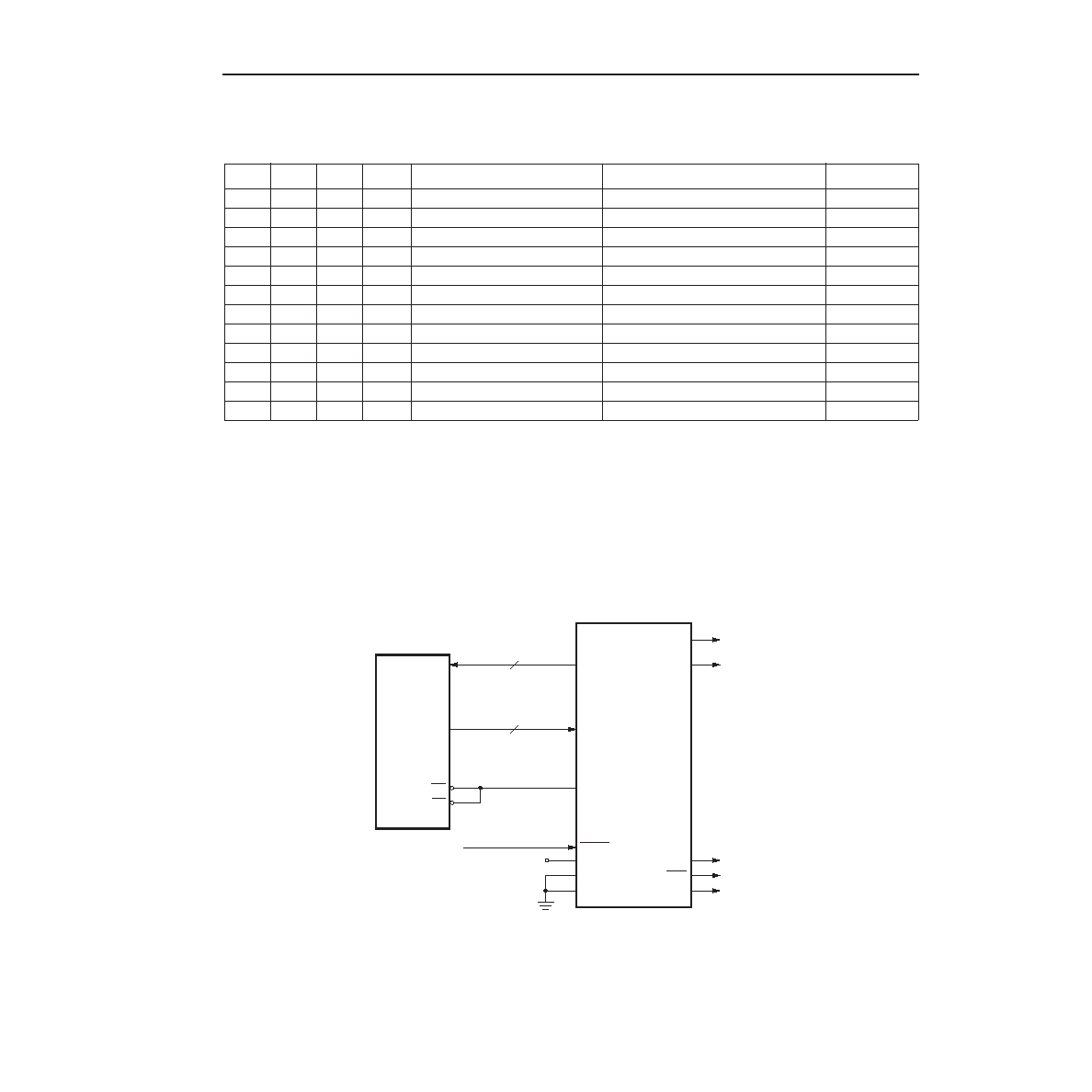
Master Parallel Mode
The master parallel conguration mode is generally used to interface to industry-standard, byte-wide memory. Fig-
ure 38 provides the connections for master parallel mode. The FPGA outputs an 22-bit address on A[21:0] to mem-
ory and reads 1 byte of conguration data on the rising edge of RCLK. The parallel bytes are internally serialized
starting with the least signicant bit, D0. D[7:0] of the FPGA can be connected to D[7:0] of the microprocessor only
if a standard prom le format is used. If a .bit or .rbt le is used from ORCA Foundry, then the user must mirror the
bytes in the .bit or .rbt le OR leave the .bit or .rbt le unchanged and connect D[7:0] of the FPGA to D[0:7] of the
microprocessor.
Note: M3 = GND for high-speed CCLK; M3 = VDD for low-frequency CCLK.
5-9738(F).a
Figure 38. Master Parallel Conguration Schematic
In master parallel mode, the starting memory address is 00000 hex, and the FPGA increments the address for each
byte loaded.
M3
M2
M1
M0
CCLK
Conguration Mode
Data
00
Output. High-frequency.
Master Serial
Serial
01
00
Output. High-frequency.
Master Parallel
8-bit
01
Output. High-frequency.
Asynchronous Peripheral
8-bit
01
11
NA
Reserved
NA
10
00
Output. Low-frequency.
Master Serial
Serial
10
01
Input.
Slave Parallel
8-bit
10
Output.
MPC860 MPI
8-bit
10
11
Output.
MPC860 MPI
16-bit
11
00
Output. Low-frequency.
Master Parallel
8-bit
11
01
Output. Low-frequency.
Asynchronous Peripheral
8-bit
11
10
Output.
MPC860 MPI
32-bit
11
Input.
Slave Serial
Serial
A[21:0]
D[7:0]
EPROM
OE
CE
PRGM
A[21:0]
D[7:0]
DONE
ORCA
SERIES
FPGA
DOUT
CCLK
HDC
LDC
RCLK
M2
M1
M0
PROGRAM
VDD
TO DAISY-
CHAINED
DEVICES
相关PDF资料 |
PDF描述 |
|---|---|
| OR4E063BA352-DB | FPGA, 2024 CLBS, 515000 GATES, PBGA352 |
| OR4E063BM680-DB | FPGA, 2024 CLBS, 515000 GATES, PBGA680 |
| ORT4622-8BC432I | FPGA, PBGA432 |
| ORT4622-8BM680I | FPGA, PBGA680 |
| ORT4622-8BC432I | FPGA, PBGA432 |
相关代理商/技术参数 |
参数描述 |
|---|---|
| OR4E10 | 制造商:AGERE 制造商全称:AGERE 功能描述:Field-Programmable Gate Arrays |
| OR4E14 | 制造商:未知厂家 制造商全称:未知厂家 功能描述:Field-Programmable Gate Arrays |
| OR4E2 | 制造商:AGERE 制造商全称:AGERE 功能描述:Field-Programmable Gate Arrays |
| OR4E2-1BA256 | 制造商:未知厂家 制造商全称:未知厂家 功能描述:FPGA |
| OR4E2-1BA352 | 制造商:未知厂家 制造商全称:未知厂家 功能描述:FPGA |
发布紧急采购,3分钟左右您将得到回复。