- 您现在的位置:买卖IC网 > PDF目录189449 > OR4E062BM680-DB (LATTICE SEMICONDUCTOR CORP) FPGA, 2024 CLBS, 515000 GATES, PBGA680 PDF资料下载
参数资料
| 型号: | OR4E062BM680-DB |
| 厂商: | LATTICE SEMICONDUCTOR CORP |
| 元件分类: | FPGA |
| 英文描述: | FPGA, 2024 CLBS, 515000 GATES, PBGA680 |
| 封装: | PLASTIC, FBGA-680 |
| 文件页数: | 126/151页 |
| 文件大小: | 2680K |
| 代理商: | OR4E062BM680-DB |
第1页第2页第3页第4页第5页第6页第7页第8页第9页第10页第11页第12页第13页第14页第15页第16页第17页第18页第19页第20页第21页第22页第23页第24页第25页第26页第27页第28页第29页第30页第31页第32页第33页第34页第35页第36页第37页第38页第39页第40页第41页第42页第43页第44页第45页第46页第47页第48页第49页第50页第51页第52页第53页第54页第55页第56页第57页第58页第59页第60页第61页第62页第63页第64页第65页第66页第67页第68页第69页第70页第71页第72页第73页第74页第75页第76页第77页第78页第79页第80页第81页第82页第83页第84页第85页第86页第87页第88页第89页第90页第91页第92页第93页第94页第95页第96页第97页第98页第99页第100页第101页第102页第103页第104页第105页第106页第107页第108页第109页第110页第111页第112页第113页第114页第115页第116页第117页第118页第119页第120页第121页第122页第123页第124页第125页当前第126页第127页第128页第129页第130页第131页第132页第133页第134页第135页第136页第137页第138页第139页第140页第141页第142页第143页第144页第145页第146页第147页第148页第149页第150页第151页
76
Lattice Semiconductor
Data Sheet
September, 2002
ORCA Series 4 FPGAs
ElectricalCharacteristics
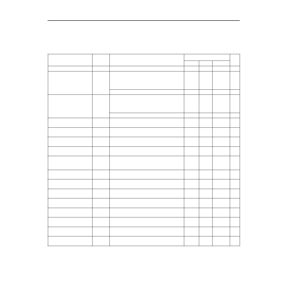
Table36.ElectricalCharacteristics
OR4ExxxIndustrial:VDD15=1.4Vto1.6V,VDD33=3.0Vto3.6V,VDDIO=3.0Vto3.6V,–40°C
<TA<+125°C;
CL= 30pF.
* Thepull-upresistorwillexternallypullthepintoalevel1.0VbelowVDDIO.
Note: 1.TheStandbyCurrentforVDDIOisvariabledependinguponI/Otypes.ForLVTTLI/OheldatVDDIOorGND,thisvalueistypicallyless
than1mA.
Parameter
Symbol
TestConditions
OR4Exxx
Unit
Min
Typ
Max
InputLeakageCurrent
IL
VDDIO=max,VIN=VSSorVDDIO
–10
—
10
A
StandbyCurrent(VDD15):
OR4E02
OR4E04
OR4E06
IDDSB15
TA=25°C,VDD15=1.6V,
VDD33
=3.6V,VDDIO=3.6V,
internaloscillatorrunning,nooutputloads,
inputsVDDIOorVSS(afterconfiguration)
—
5
10
15
200
mA
SameconditionsexceptTA=85°C
—
500
mA
StandbyCurrent(VDD33):
OR4E02
OR4E04
OR4E06
IDDSB33
TA=25°C,VDD15=1.6V,
VDD33
=3.6V,VDDIO=3.6V,
internaloscillatorstopped,nooutputloads,
inputsVDDIOorGND(afterconfiguration)
—
4
7
10
100
mA
SameconditionsexceptTA=85°C
—
300
mA
DataRetentionVoltage
(VDD33)
VDR33
TJ=–40°Cto125°C
2.3
—
V
DataRetentionVoltage
(VDD15)
VDR15
TJ=–40°Cto125°C
1.1
—
V
DCInputLevels
VIL
VIH
Inputlevelsvaryperinputstandard.Seethe
Series4IOApplicationNotefordetails
Various
—
Various
V
DCOutputLevels
VOL
VOH
Outputlevelsvaryperoutputstandard.See
theSeries4IOApplicationNotefordetails
Various
—
Various
V
OutputDriveCurrents
IOL
IOH
Outputcurrentsvaryperoutputstandard.
SeetheSeries4IOApplicationNotefor
details
Various
—
Various
mA
InputCapacitance
CIN
TA=25°C,VDDIO=3.6V,
Testfrequency=1MHz
——
5
pF
OutputCapacitance
COUT
TA=25°C,VDDIO=3.6V,
Testfrequency=1MHz
——
5
pF
DONEPull-up
Resistor*
RDONE
VDDIO=3.0Vto3.6V,VIN=VSS,
TJ=–40°Cto125°C
100
—
k
M[3:0]Pull-up
Resistors*
RM
VDDIO=3.0Vto3.6V,VIN=VSS,
TJ=–40°Cto125°C
100
—
k
I/OPadStaticPull-up
Current*
IPU
VDDIO=3.0Vto3.6V,VIN=VSS,
TJ=–40°Cto125°C
14.4
—
50.9
A
I/OPadStatic
Pull-downCurrent
IPD
VDDIO=3.0Vto3.6V,VIN=VSS,
TJ=–40°Cto125°C
26
—
103
A
I/OPadPull-up
Resistor*
RPU
VDDIO=3.0Vto3.6V,VIN=VSS,
TJ=–40°Cto125°C
100
—
k
I/OPadPull-down
Resistor
RPD
VDDIO=3.0Vto3.6V,VIN=VDD,
TJ=–40°Cto125°C
50
—
k
相关PDF资料 |
PDF描述 |
|---|---|
| OR4E063BA352-DB | FPGA, 2024 CLBS, 515000 GATES, PBGA352 |
| OR4E063BM680-DB | FPGA, 2024 CLBS, 515000 GATES, PBGA680 |
| ORT4622-8BC432I | FPGA, PBGA432 |
| ORT4622-8BM680I | FPGA, PBGA680 |
| ORT4622-8BC432I | FPGA, PBGA432 |
相关代理商/技术参数 |
参数描述 |
|---|---|
| OR4E10 | 制造商:AGERE 制造商全称:AGERE 功能描述:Field-Programmable Gate Arrays |
| OR4E14 | 制造商:未知厂家 制造商全称:未知厂家 功能描述:Field-Programmable Gate Arrays |
| OR4E2 | 制造商:AGERE 制造商全称:AGERE 功能描述:Field-Programmable Gate Arrays |
| OR4E2-1BA256 | 制造商:未知厂家 制造商全称:未知厂家 功能描述:FPGA |
| OR4E2-1BA352 | 制造商:未知厂家 制造商全称:未知厂家 功能描述:FPGA |
发布紧急采购,3分钟左右您将得到回复。