- 您现在的位置:买卖IC网 > PDF目录189449 > OR4E062BM680-DB (LATTICE SEMICONDUCTOR CORP) FPGA, 2024 CLBS, 515000 GATES, PBGA680 PDF资料下载
参数资料
| 型号: | OR4E062BM680-DB |
| 厂商: | LATTICE SEMICONDUCTOR CORP |
| 元件分类: | FPGA |
| 英文描述: | FPGA, 2024 CLBS, 515000 GATES, PBGA680 |
| 封装: | PLASTIC, FBGA-680 |
| 文件页数: | 76/151页 |
| 文件大小: | 2680K |
| 代理商: | OR4E062BM680-DB |
第1页第2页第3页第4页第5页第6页第7页第8页第9页第10页第11页第12页第13页第14页第15页第16页第17页第18页第19页第20页第21页第22页第23页第24页第25页第26页第27页第28页第29页第30页第31页第32页第33页第34页第35页第36页第37页第38页第39页第40页第41页第42页第43页第44页第45页第46页第47页第48页第49页第50页第51页第52页第53页第54页第55页第56页第57页第58页第59页第60页第61页第62页第63页第64页第65页第66页第67页第68页第69页第70页第71页第72页第73页第74页第75页当前第76页第77页第78页第79页第80页第81页第82页第83页第84页第85页第86页第87页第88页第89页第90页第91页第92页第93页第94页第95页第96页第97页第98页第99页第100页第101页第102页第103页第104页第105页第106页第107页第108页第109页第110页第111页第112页第113页第114页第115页第116页第117页第118页第119页第120页第121页第122页第123页第124页第125页第126页第127页第128页第129页第130页第131页第132页第133页第134页第135页第136页第137页第138页第139页第140页第141页第142页第143页第144页第145页第146页第147页第148页第149页第150页第151页
30
Lattice Semiconductor
Data Sheet
September, 2002
ORCA Series 4 FPGAs
Embedded Block RAM (continued)
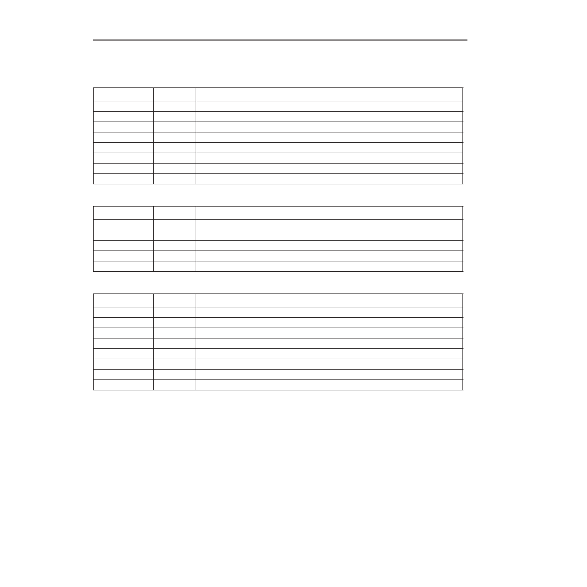
Table 10. Constant Multiplier Signals
Table 11. 8x8 Multiplier Signals
Table 12. CAM Signals
Port Signals
I/O
Function
AR0[15:0]
I
Data input–operand.
AW(1:0)[8:0]
I
Address bits.
D(1:0)[17:0]
I
Data inputs to load memory or change coefcient.
CKW[0:1]
I
Positive-edge write port clock.
CKR[0:1]
I
Positive-edge read port clock. Used for synchronous multiply mode.
CSW[1:0]
I
Active-high write enable.
CSR[1:0]
I
Active-high read enable.
Q[23:0]
O
Data outputs–product result.
Port Signals
I/O
Function
AR0[7:0]
I
Data input-Multiplicand.
AR1[7:0]
I
Data input-Multiplier.
CKR[0:1]
I
Positive-edge read port clock. Used for synchronous multiply mode.
CSR[1:0]
I
Active-high read enable.
Q[15:0]
O
Data outputs-product.
Port Signals
I/O
Function
AR(1:0)[7:0]
I
Data Match.
AW(1:0)[8:0]
I
Data Write.
D(1:0)[17]
I
Clear data active high.
D(1:0)[16]
I
Single match active high.
D(1:0)[3:0]
I
CAM address for data write.
CSW[1:0]
I
Active-high write enable. Enable for CAM data write.
CSR[1:0]
I
Active-high read enable. Enable for CAM data match.
Q(1:0)15:0]
O
Decoded Data outputs. “1” corresponds to a data match at that address location.
相关PDF资料 |
PDF描述 |
|---|---|
| OR4E063BA352-DB | FPGA, 2024 CLBS, 515000 GATES, PBGA352 |
| OR4E063BM680-DB | FPGA, 2024 CLBS, 515000 GATES, PBGA680 |
| ORT4622-8BC432I | FPGA, PBGA432 |
| ORT4622-8BM680I | FPGA, PBGA680 |
| ORT4622-8BC432I | FPGA, PBGA432 |
相关代理商/技术参数 |
参数描述 |
|---|---|
| OR4E10 | 制造商:AGERE 制造商全称:AGERE 功能描述:Field-Programmable Gate Arrays |
| OR4E14 | 制造商:未知厂家 制造商全称:未知厂家 功能描述:Field-Programmable Gate Arrays |
| OR4E2 | 制造商:AGERE 制造商全称:AGERE 功能描述:Field-Programmable Gate Arrays |
| OR4E2-1BA256 | 制造商:未知厂家 制造商全称:未知厂家 功能描述:FPGA |
| OR4E2-1BA352 | 制造商:未知厂家 制造商全称:未知厂家 功能描述:FPGA |
发布紧急采购,3分钟左右您将得到回复。