- 您现在的位置:买卖IC网 > PDF目录98081 > SII3531ACNU PCI BUS CONTROLLER, QCC48 PDF资料下载
参数资料
| 型号: | SII3531ACNU |
| 元件分类: | 总线控制器 |
| 英文描述: | PCI BUS CONTROLLER, QCC48 |
| 封装: | 7 X 7 MM, 0.40 MM PITCH, LEAD FREE, QFN-48 |
| 文件页数: | 75/81页 |
| 文件大小: | 532K |
| 代理商: | SII3531ACNU |
第1页第2页第3页第4页第5页第6页第7页第8页第9页第10页第11页第12页第13页第14页第15页第16页第17页第18页第19页第20页第21页第22页第23页第24页第25页第26页第27页第28页第29页第30页第31页第32页第33页第34页第35页第36页第37页第38页第39页第40页第41页第42页第43页第44页第45页第46页第47页第48页第49页第50页第51页第52页第53页第54页第55页第56页第57页第58页第59页第60页第61页第62页第63页第64页第65页第66页第67页第68页第69页第70页第71页第72页第73页第74页当前第75页第76页第77页第78页第79页第80页第81页
PCI Express to Serial ATA Controller
Data Sheet
Silicon Image, Inc.
2006 Silicon Image, Inc.
SiI-DS-0208-C
77
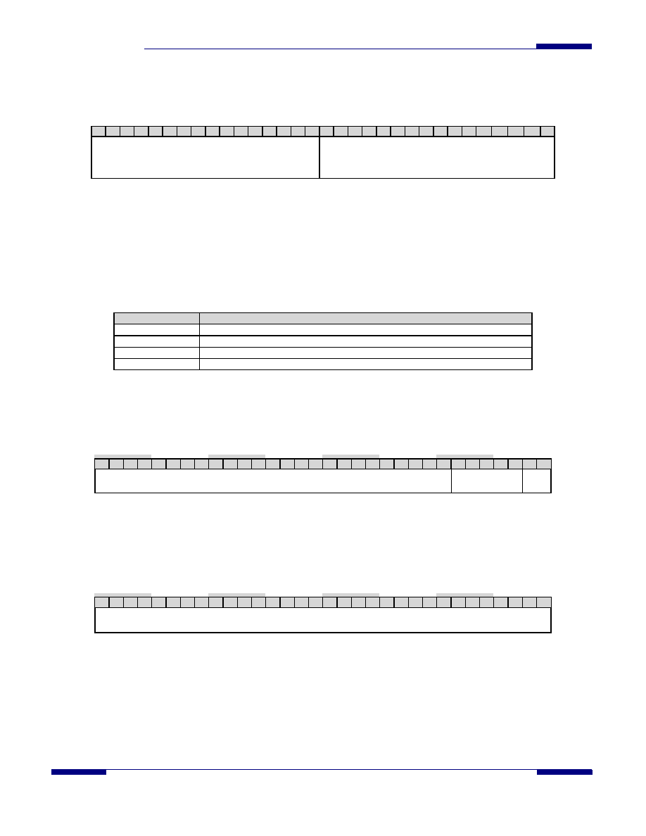
6.3.24 SNotification
Address Offset: 1F10H
Access Type: Read/Write 1 to Clear
Reset Value: 0x0000_0000
31 30 29 28 27 26 25 24 23 22 21 20 19 18 17 16 15 14 13 12 11 10 09 08 07 06 05 04 03 02 01 00
Reserved
Notify bits
This register reports the devices that have sent a Set Device Bits FIS with the Notification bit set.
Bit [31:16]: Reserved (R). This bit field is reserved and returns zeros on a read.
Bit [15:00]: Notify bits (R/W1C) – These 16 bits correspond to the 16 possible devices connected to a Port
Multiplier on this port.
6.4 Internal Register Space – Base Address 2
These registers are 32-bits wide and provide Indirect Register Access to the registers of the SiI3531A. Access to this register
space is through the PCI I/O space.
Address Offset
Register Name
00H
Global Register Offset
04H
Global Register Data
08H
Port Register Offset
0CH
Port Register Data
Table 6-11 SiI3531A Internal Register Space – Base Address 2
6.4.1
Global Register Offset
Address Offset: 00H
Access Type: Read/Write
Reset Value: 0x0000_0000
31 30 29 28 27 26 25 24 23 22 21 20 19 18 17 16 15 14 13 12 11 10 09 08 07 06 05 04 03 02 01 00
Reserved
Dword Offset
00
This register provides indirect addressing of a Global Register otherwise accessible directly via Base Address Register 0. The
Dword address offset for an indirect access is in bits 6 to 2; bits 31 to 7, 1, and 0 are reserved and should always be 0.
Indirect access is not allowed to the Global registers at offsets 0x78 through 0x7F (Configuration register indirect access).
6.4.2
Global Register Data
Address Offset: 04H
Access Type: Read/Write
31 30 29 28 27 26 25 24 23 22 21 20 19 18 17 16 15 14 13 12 11 10 09 08 07 06 05 04 03 02 01 00
As defined for indirectly accessed register
This register provides the indirect access addressed by the Global Register Offset register.
相关PDF资料 |
PDF描述 |
|---|---|
| SIO10N268-NU | MULTIFUNCTION PERIPHERAL, PQFP128 |
| SIS300 | GRAPHICS PROCESSOR, PBGA365 |
| SK12430PJT | 800 MHz, OTHER CLOCK GENERATOR, PQCC28 |
| SK12439PJ | 800 MHz, OTHER CLOCK GENERATOR, PQCC28 |
| SK12439PJT | 800 MHz, OTHER CLOCK GENERATOR, PQCC28 |
相关代理商/技术参数 |
参数描述 |
|---|---|
| SII3611 | 制造商:SILICONIMAGE 制造商全称:SILICONIMAGE 功能描述:SATALink Device Bridge |
| SII3611CT80-1.5 | 制造商:SILICON IMAGE 功能描述:3611CT80-1.5 |
| SII3723 | 制造商:SILICONIMAGE 制造商全称:SILICONIMAGE 功能描述:Third Generation SATA Port Multiplier Storage Processor |
| SiI3723CNU | 制造商:Silicon Image Inc 功能描述: |
| SII3726 | 制造商:SILICONIMAGE 制造商全称:SILICONIMAGE 功能描述:SATA Port Multiplier |
发布紧急采购,3分钟左右您将得到回复。