- 您现在的位置:买卖IC网 > PDF目录68583 > WJLXT384LEB1 (CORTINA SYSTEMS INC) DATACOM, PCM TRANSCEIVER, PQFP144 PDF资料下载
参数资料
| 型号: | WJLXT384LEB1 |
| 厂商: | CORTINA SYSTEMS INC |
| 元件分类: | 数字传输电路 |
| 英文描述: | DATACOM, PCM TRANSCEIVER, PQFP144 |
| 封装: | 20 X 20MM, ROHS COMPLIANT, LQFP-144 |
| 文件页数: | 65/140页 |
| 文件大小: | 1514K |
| 代理商: | WJLXT384LEB1 |
第1页第2页第3页第4页第5页第6页第7页第8页第9页第10页第11页第12页第13页第14页第15页第16页第17页第18页第19页第20页第21页第22页第23页第24页第25页第26页第27页第28页第29页第30页第31页第32页第33页第34页第35页第36页第37页第38页第39页第40页第41页第42页第43页第44页第45页第46页第47页第48页第49页第50页第51页第52页第53页第54页第55页第56页第57页第58页第59页第60页第61页第62页第63页第64页当前第65页第66页第67页第68页第69页第70页第71页第72页第73页第74页第75页第76页第77页第78页第79页第80页第81页第82页第83页第84页第85页第86页第87页第88页第89页第90页第91页第92页第93页第94页第95页第96页第97页第98页第99页第100页第101页第102页第103页第104页第105页第106页第107页第108页第109页第110页第111页第112页第113页第114页第115页第116页第117页第118页第119页第120页第121页第122页第123页第124页第125页第126页第127页第128页第129页第130页第131页第132页第133页第134页第135页第136页第137页第138页第139页第140页
30
Document Number: 248994
Revision Number: 005
Revision Date: November 28, 2005
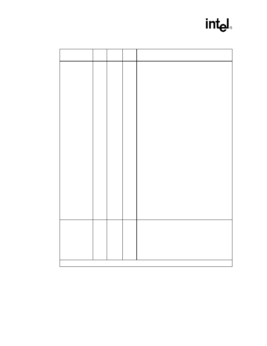
Intel LXT384 Octal T1/E1/J1 S/H PCM Transceiver with JA
BPV7 / RNEG7
BPV6 / RNEG6
BPV5 / RNEG5
BPV4 / RNEG4
BPV3 / RNEG3
BPV2 / RNEG2
BPV1 / RNEG1
BPV0 / RNEG0
141
4
105
112
69
76
34
41
A3
C3
C12
A12
P12
M12
M3
P3
DO
Receive Negative Data Output 7:0.
This signal description applies to both RNEG and RPOS in
bipolar I/O mode. When the LXT384 Transceiver is in the:
Host processor mode, during an LOS condition, AIS
can be inserted into the receive path. See the
description of the GCR register RAISEN bit, in Section
Hardware mode, RNEG and RPOS remain active
during an LOS condition.
When MCLK is provided with a clocking signal:
The LXT384 Transceiver enters clock-recovery mode.
RNEG[7:0] act as active-high bipolar Non Return to
Zero (NRZ) receive signal outputs.
A High signal on RNEG corresponds to receipt of a
negative pulse on RTIP/RRING.
A High signal on RPOS corresponds to receipt of a
positive pulse on RTIP/RRING.
These signals are valid on the falling or rising edges of
RCLK, depending on the CLKE input. See the CLKE
pin description in Table 11, “Clocks and Clock-Related
When MCLK is high:
The LXT384 Transceiver enters data recovery mode.
RNEG[7:0] act as RZ data receiver outputs.
These signals are valid on the falling or rising edges of
RCLK, depending on the CLKE input. See the CLKE
pin description in Table 11, “Clocks and Clock-Related
When MCLK is low:
RNEG and RPOS can be placed in a high-impedance
tristate with the MCLK pin. (For details, see MCLK in
NOTE: For pin functions involving unipolar mode, see the
BPV pin description.
RDATA7 / RPOS7
RDATA6 / RPOS6
RDATA5 / RPOS5
RDATA4 / RPOS4
RDATA3 / RPOS3
RDATA2 / RPOS2
RDATA1 / RPOS1
RDATA0 / RPOS0
142
5
104
111
70
77
33
40
A2
C2
C13
A13
P13
M13
M2
P2
DO
Receive Positive Data Output 7:0.
For the RPOS description, see RNEG.
NOTE: For pin functions involving unipolar mode, see the
RDATA pin description.
Table 8.
Framer/Mapper Receive Signals (Sheet 2 of 2)
Signal
Name
QFP
Pin
PBGA
Ball
Signal
Type
Signal Description
1. AI: Analog Input. AO: Analog Output. DI: Digital Input. DI/O: Digital Bidirectional Port. DO: Digital Output.
相关PDF资料 |
PDF描述 |
|---|---|
| WJLXT385LEB1 | DATACOM, PCM TRANSCEIVER, PQFP144 |
| WJLXT385LEB1 | DATACOM, PCM TRANSCEIVER, PQFP144 |
| WJLXT386LEB2 | DATACOM, PCM TRANSCEIVER, PQFP100 |
| WJLXT386LEB2 | DATACOM, PCM TRANSCEIVER, PQFP100 |
| WJLXT388LEB2 | DATACOM, PCM TRANSCEIVER, PQFP100 |
相关代理商/技术参数 |
参数描述 |
|---|---|
| WJLXT386LE.B2 | 功能描述:IC TRANS QUAD T1/E1/J1 100-LQFP RoHS:是 类别:集成电路 (IC) >> 接口 - 驱动器,接收器,收发器 系列:- 产品培训模块:Lead (SnPb) Finish for COTS Obsolescence Mitigation Program 标准包装:25 系列:- 类型:收发器 驱动器/接收器数:2/2 规程:RS232 电源电压:4.5 V ~ 5.5 V 安装类型:通孔 封装/外壳:16-DIP(0.300",7.62mm) 供应商设备封装:16-PDIP 包装:管件 |
| WJLXT6155LE.B5 | 制造商:Intel 功能描述:SONET/SDH/ATM Transceiver 1TX 1RX 64-Pin LQFP |
| WJLXT6155LE.B5-866255 | 功能描述:TXRX SDH/SONET/ATM HS 64-LQFP RoHS:是 类别:集成电路 (IC) >> 接口 - 驱动器,接收器,收发器 系列:- 产品培训模块:Lead (SnPb) Finish for COTS Obsolescence Mitigation Program 标准包装:50 系列:- 类型:收发器 驱动器/接收器数:1/1 规程:RS422,RS485 电源电压:4.75 V ~ 5.25 V 安装类型:通孔 封装/外壳:8-DIP(0.300",7.62mm) 供应商设备封装:8-PDIP 包装:管件 产品目录页面:1402 (CN2011-ZH PDF) |
| WJLXT6155LE.B5-866256 | 制造商:Cortina Systems Inc 功能描述:SONET/SDH/ATM Transceiver 1TX 1RX 64-Pin LQFP T/R |
| WJLXT901ALC.A4 | 功能描述:IC 10BASE-T/AUI TXCVR 64-LQFP RoHS:是 类别:集成电路 (IC) >> 接口 - 驱动器,接收器,收发器 系列:- 标准包装:1,000 系列:- 类型:收发器 驱动器/接收器数:2/2 规程:RS232 电源电压:3 V ~ 5.5 V 安装类型:表面贴装 封装/外壳:16-SOIC(0.295",7.50mm 宽) 供应商设备封装:16-SOIC 包装:带卷 (TR) |
发布紧急采购,3分钟左右您将得到回复。