- 您现在的位置:买卖IC网 > PDF目录378250 > 865G (Intel Corp.) Intel 865G/865GV Graphics and Memory Controller Hub PDF资料下载
参数资料
| 型号: | 865G |
| 厂商: | Intel Corp. |
| 英文描述: | Intel 865G/865GV Graphics and Memory Controller Hub |
| 中文描述: | 英特尔865G/865GV图形和内存控制器中枢 |
| 文件页数: | 100/249页 |
| 文件大小: | 3540K |
| 代理商: | 865G |
第1页第2页第3页第4页第5页第6页第7页第8页第9页第10页第11页第12页第13页第14页第15页第16页第17页第18页第19页第20页第21页第22页第23页第24页第25页第26页第27页第28页第29页第30页第31页第32页第33页第34页第35页第36页第37页第38页第39页第40页第41页第42页第43页第44页第45页第46页第47页第48页第49页第50页第51页第52页第53页第54页第55页第56页第57页第58页第59页第60页第61页第62页第63页第64页第65页第66页第67页第68页第69页第70页第71页第72页第73页第74页第75页第76页第77页第78页第79页第80页第81页第82页第83页第84页第85页第86页第87页第88页第89页第90页第91页第92页第93页第94页第95页第96页第97页第98页第99页当前第100页第101页第102页第103页第104页第105页第106页第107页第108页第109页第110页第111页第112页第113页第114页第115页第116页第117页第118页第119页第120页第121页第122页第123页第124页第125页第126页第127页第128页第129页第130页第131页第132页第133页第134页第135页第136页第137页第138页第139页第140页第141页第142页第143页第144页第145页第146页第147页第148页第149页第150页第151页第152页第153页第154页第155页第156页第157页第158页第159页第160页第161页第162页第163页第164页第165页第166页第167页第168页第169页第170页第171页第172页第173页第174页第175页第176页第177页第178页第179页第180页第181页第182页第183页第184页第185页第186页第187页第188页第189页第190页第191页第192页第193页第194页第195页第196页第197页第198页第199页第200页第201页第202页第203页第204页第205页第206页第207页第208页第209页第210页第211页第212页第213页第214页第215页第216页第217页第218页第219页第220页第221页第222页第223页第224页第225页第226页第227页第228页第229页第230页第231页第232页第233页第234页第235页第236页第237页第238页第239页第240页第241页第242页第243页第244页第245页第246页第247页第248页第249页
Intel
82865G/82865GV GMCH Datasheet
101
Register Description
3.7
Integrated Graphics Device Registers (Device 2)
Function 0 can be VGA compatible or not; this is selected through GC[bit 1] (offset 52, Device 0).
This section contains the Integrated Graphics Device PCI configuration registers listed in order of
ascending offset address. The register address map is shown in
Table 10
.
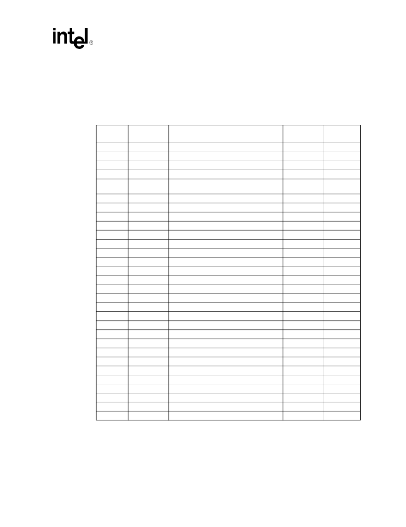
Table 10. Integrated Graphics Device PCI Register Address Map (Device 2)
Address
Offset
Register
Symbol
Register Name
Default Value
Access
00–01h
VID2
Vendor Identification
8086h
RO
02–03h
DID2
Device Identification
2572h
RO
04–05h
PCICMD2
PCI Command
0000h
RO,R/W
06–07h
PCISTS2
PCI Status
0090h
RO,R/WC
08h
RID2
Revision Identification
See register
description
RO
09–0Bh
CC
Class Code
030000h
RO
0Ch
CLS
Cache Line Size
00h
RO
0Dh
MLT2
Master Latency Timer
00h
RO
0Eh
HDR2
Header Type
00h
RO
0Fh
—
Intel Reserved
—
—
10–13h
GMADR
Graphics Memory Range Address
00000008h
R/W,RO
14–17h
MMADR
Memory-Mapped Range Address
00000000h
R/W,RO
18–1Bh
IOBAR
IO Decode
00000000h
R/W
1C–2Bh
—
Reserved
—
—
2C–2Dh
SVID2
Subsystem Vendor Identification
0000h
R/WO
2E–2Fh
SID2
Subsystem Identification
0000h
R/WO
30–33h
ROMADR
Video BIOS ROM Base Address
00000000h
RO
34h
CAPPOINT
Capabilities Pointer
D0h
RO
35–3Bh
—
Reserved
—
—
3Ch
INTRLINE
Interrupt Line
00h
R/W, RO
3Dh
INTRPIN
Interrupt Pin
01h
RO
3Eh
MINGNT
Minimum Grant
00h
RO
3Fh
MAXLAT
Maximum Latency
00h
RO
40–CFh
—
Intel Reserved
00h
—
D0–D1h
PMCAPID
Power Management Capabilities ID
0001h
RO
D2–D3h
PMCAP
Power Management Capabilities
0021h
RO
D4–D5h
PMCS
Power Management Control
0000h
R/W,RO
D6–DFh
—
Intel Reserved
—
—
E0–E1h
SWSMI
Software SMI Interface
0000h
R/W
E2–FFh
—
Intel Reserved
—
—
相关PDF资料 |
PDF描述 |
|---|---|
| 8663 | T-1 Subminiature Lamps |
| 8664 | T-1 Subminiature Lamps |
| 8666 | T- Subminiature Lamps |
| 86HF160 | STANDARD RECOVERY DIODES |
| 86HF120M | STANDARD RECOVERY DIODES |
相关代理商/技术参数 |
参数描述 |
|---|---|
| 865G NEO2-LS | 制造商:Micro-Star International 功能描述:865G P4 ATX 800FSB VID - Bulk |
| 865GM2-LS | 制造商:Micro-Star International 功能描述:INTEL P4 800FSB MOTHERBOARD - Bulk |
| 865GV | 制造商:INTEL 制造商全称:Intel Corporation 功能描述:Intel 865G/865GV Graphics and Memory Controller Hub |
| 865GVM3-V | 制造商:Micro-Star International 功能描述:MSI 865GVM3-V MOTHERBOARD - Bulk |
| 865GVM3-V RPL | 制造商:Micro-Star International 功能描述:REPAIR/REPLACEMENT - Bulk |
发布紧急采购,3分钟左右您将得到回复。