- 您现在的位置:买卖IC网 > PDF目录224693 > PC87393F-VJG (NATIONAL SEMICONDUCTOR CORP) 100-Pin LPC SuperI/O Devices for Portable Applications PDF资料下载
参数资料
| 型号: | PC87393F-VJG |
| 厂商: | NATIONAL SEMICONDUCTOR CORP |
| 元件分类: | 外设及接口 |
| 英文描述: | 100-Pin LPC SuperI/O Devices for Portable Applications |
| 中文描述: | MULTIFUNCTION PERIPHERAL, PQFP100 |
| 封装: | TQFP-100 |
| 文件页数: | 10/148页 |
| 文件大小: | 1733K |
| 代理商: | PC87393F-VJG |
第1页第2页第3页第4页第5页第6页第7页第8页第9页当前第10页第11页第12页第13页第14页第15页第16页第17页第18页第19页第20页第21页第22页第23页第24页第25页第26页第27页第28页第29页第30页第31页第32页第33页第34页第35页第36页第37页第38页第39页第40页第41页第42页第43页第44页第45页第46页第47页第48页第49页第50页第51页第52页第53页第54页第55页第56页第57页第58页第59页第60页第61页第62页第63页第64页第65页第66页第67页第68页第69页第70页第71页第72页第73页第74页第75页第76页第77页第78页第79页第80页第81页第82页第83页第84页第85页第86页第87页第88页第89页第90页第91页第92页第93页第94页第95页第96页第97页第98页第99页第100页第101页第102页第103页第104页第105页第106页第107页第108页第109页第110页第111页第112页第113页第114页第115页第116页第117页第118页第119页第120页第121页第122页第123页第124页第125页第126页第127页第128页第129页第130页第131页第132页第133页第134页第135页第136页第137页第138页第139页第140页第141页第142页第143页第144页第145页第146页第147页第148页
7.0 X-Bus Extension (Continued)
107
www.national.com
The X-Bus interface outputs the address in one of two modes:
q
Normal Address mode - A pin is assigned for each address line, and a non-multiplexed address data bus is used.
q
Latched Address mode - The number of pins used for outputting the address is reduced. The address lines are mul-
tiplexed with the data bus. External latches should be used to enable the memory or I/O device access to the multi-
plexed address signals. When the memory conguration uses more than 1 Mbyte of memory, this mode must be
used to generate address signals 20 through 27.
X-Bus access timing is driven by an internal version of the LPC clock (i.e., it has the same frequency but may have some
phase delay), referred to in this section simply as "the clock". The transactions are described in reference to the clock, and
the AC specications are relative to it. This provides an easy way for calculating the timing for the system design. However,
the system interface is optimized for an asynchronous interface. For hints on how to use it, refer to the usage hints in Section
7.3.1
Programmable I/O Range Chip Select
The PC8739x has two chip select signals, XCS1-0, to indicate X-Bus accesses. The PC8739x X-Bus functional block en-
ables flexible association of these chip selects with I/O and memory address ranges in the LPC address space. The Chip
Select Mapping field of the X-Bus Zone Configuration registers defines to which of the decoded address ranges the respec-
tive XCS signal responds. In addition, the X-Bus Configuration register enables specifying the access time for the respective
select signal via bits that control the fixed wait cycles and variable wait cycles, using the XRDY input.
If the chip select signal setting results in a conflict in which both selects are configured for the same transaction, XCS0 has
priority. XCS1 remains inactive and its Configuration register setting is ignored. For zones that are not associated with one
of the chip select signals, the X-Bus does not respond to LPC transactions.
7.3.2
LPC and FWH Address to X-Bus Address Translation
The BIOS memory on the LPC bus can occupy one of three regions in the memory space (specified in Table 29 and Table
31). Address translation between the LPC bus address and the X-Bus is performed as follows:
I/O Transactions. The 16-bit address of the LPC bus is padded with zeroes (bits 16 through 27) to create the 28-bit input
address to the X-Bus functional block.
Memory Transactions. The 32-bit address received from the LPC bus is used to decode the different zones described in
Section 2.19. The address is then translated to the X-Bus address using the following rules:
q
User-Dened Zone (UDZ) and 386 Mode-Compatible BIOS Range (LPC or LPC-FWH) - The 28 least signicant bits
of the LPC address are used as the X-Bus input address. Figure 22 illustrates the mapping for this zone. (Note: See
Section 2.8.1 for the way addresses are built for FWH transactions.)
q
Legacy and Extended Legacy BIOS Range - The 17 least signicant bits (A16-0) of the LPC address are routed as
the 17 least signicant signals address lines of the X-Bus (XA16-0). The upper 11 X-Bus address lines are driven to
1. This shifts the addresses to the end of the X-Bus memory space (see Figure 23).
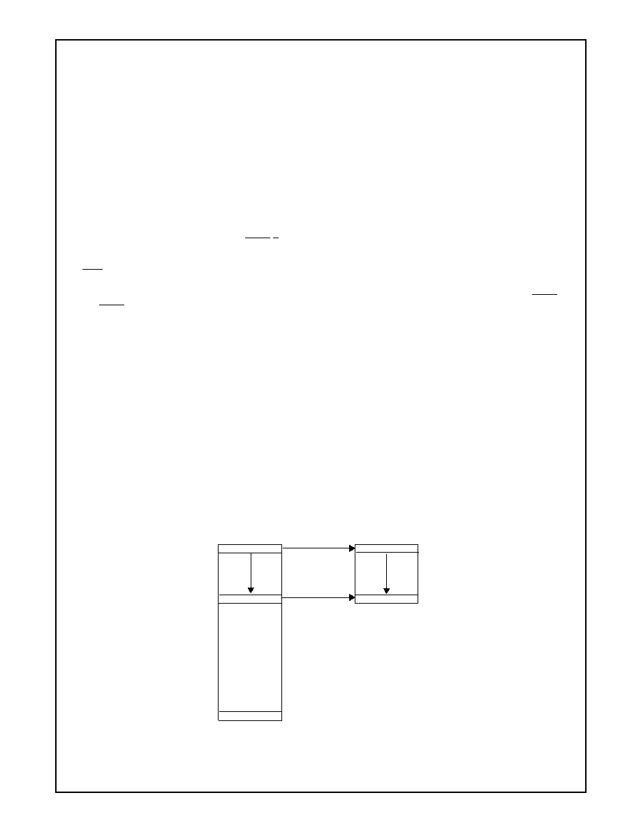
Figure 22. LPC to X-Bus Address Translation: 386 Mode-Compatible BIOS Range
LPC Bus Address
FFFFFFFFh
xFFFFFFFh
X-Bus Address
FFC00000h
xFC00000h
00000000h
**
*
相关PDF资料 |
PDF描述 |
|---|---|
| PC906N | 896 MHz - 940 MHz YAGI ANTENNA, 10.65 dBi GAIN, 65 deg 3dB BEAMWIDTH |
| PC926N | 928 MHz - 960 MHz YAGI ANTENNA, 10.65 dBi GAIN, 65 deg 3dB BEAMWIDTH |
| PCA.1D.694.CNAD42Z | CABLE TERMINATED, FEMALE, RF CONNECTOR, SOCKET |
| PCA.1D.694.CNAD42 | CABLE TERMINATED, FEMALE, RF CONNECTOR, SOCKET |
| PCA.1D.694.CNAD52Z | CABLE TERMINATED, FEMALE, RF CONNECTOR, SOCKET |
相关代理商/技术参数 |
参数描述 |
|---|---|
| PC87393VJG | 制造商:Texas Instruments 功能描述: 制造商:Texas Instruments 功能描述:IC, SUPER I/O DEVICE, TQFP-100, Logic Device Type:Buffer, Supply Voltage Min:3V, |
| PC87393-VJG | 制造商:NSC 制造商全称:National Semiconductor 功能描述:100-Pin LPC SuperI/O Devices for Portable Applications |
| PC87410 | 制造商:NSC 制造商全称:National Semiconductor 功能描述:PC87410 PCI-IDE Interface Controller |
| PC87410VLK | 制造商:Rochester Electronics LLC 功能描述:- Bulk |
| PC87413 | 制造商:NSC 制造商全称:National Semiconductor 功能描述:LPC ServerI/O for Servers and Workstations |
发布紧急采购,3分钟左右您将得到回复。