- 您现在的位置:买卖IC网 > PDF目录224693 > PC87393F-VJG (NATIONAL SEMICONDUCTOR CORP) 100-Pin LPC SuperI/O Devices for Portable Applications PDF资料下载
参数资料
| 型号: | PC87393F-VJG |
| 厂商: | NATIONAL SEMICONDUCTOR CORP |
| 元件分类: | 外设及接口 |
| 英文描述: | 100-Pin LPC SuperI/O Devices for Portable Applications |
| 中文描述: | MULTIFUNCTION PERIPHERAL, PQFP100 |
| 封装: | TQFP-100 |
| 文件页数: | 14/148页 |
| 文件大小: | 1733K |
| 代理商: | PC87393F-VJG |
第1页第2页第3页第4页第5页第6页第7页第8页第9页第10页第11页第12页第13页当前第14页第15页第16页第17页第18页第19页第20页第21页第22页第23页第24页第25页第26页第27页第28页第29页第30页第31页第32页第33页第34页第35页第36页第37页第38页第39页第40页第41页第42页第43页第44页第45页第46页第47页第48页第49页第50页第51页第52页第53页第54页第55页第56页第57页第58页第59页第60页第61页第62页第63页第64页第65页第66页第67页第68页第69页第70页第71页第72页第73页第74页第75页第76页第77页第78页第79页第80页第81页第82页第83页第84页第85页第86页第87页第88页第89页第90页第91页第92页第93页第94页第95页第96页第97页第98页第99页第100页第101页第102页第103页第104页第105页第106页第107页第108页第109页第110页第111页第112页第113页第114页第115页第116页第117页第118页第119页第120页第121页第122页第123页第124页第125页第126页第127页第128页第129页第130页第131页第132页第133页第134页第135页第136页第137页第138页第139页第140页第141页第142页第143页第144页第145页第146页第147页第148页
7.0 X-Bus Extension (Continued)
110
www.national.com
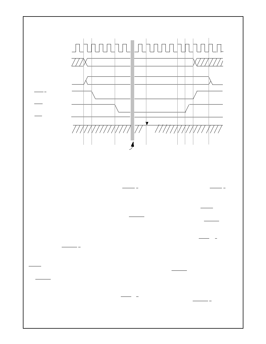
Figure 25. Write Access Cycle - Normal Address Mode
7.3.6
Latched Address Mode X-Bus Transactions
The read and write transactions in Latched address mode are similar to those used in Normal address mode, except for how
the addresses are placed on the X-Bus. In this mode, address signals 27-0 are output using the XA signals and via multi-
plexing over the data bus (XD7-0). Latch control signals XSTB2-0 help a system capture these signals. The XSTB2-0 signals
are placed as long as the address signal are valid (until the end of a transaction).
Once a read cycle on the LPC falls within the range of any of the enabled X-Bus decoded address ranges, a read cycle
begins. A read cycle starts by outputting the lower twenty address signals on address signals XA19-0, and address signals
27-20 on data signals XD7-0, on the rising edge of the clock. Two clock cycles later, a strobe signal (XSTB2) is asserted to
latch the information on an external latch. Two clock cycles later, a second set of address signals, 19-12, is placed on data
pins XD7-0. These may be latched using the strobe signal XSTRB1 output two cycles later on the rising edge of the clock.
Two clock cycles later, the last group of address signals, 11-4, is output on data signals XD7-0. The XSTRB0 output two
cycles later, on the rising edge of the clock, may be used to latch this part of the address. Two cycles later on the rising edge
of the clock, the PC8739x stops driving the data bus. At this point, all addresses are available either on the address outputs
of the PC8739x (XA19-0) or in one of the three latches. The system may require only part of these addresses, depending
on the size of the address memory or peripheral space. One clock cycle later, a chip select signal XCS1 or 0 is asserted,
based on the address accessed and the select signal mapping. From this point, the read continues as described for the Nor-
mal address mode. XSTRB2-0 are deasserted when the address becomes invalid.
Once a write cycle on the LPC falls within the range of any of the enabled decoded address ranges of the X-Bus functional
block, a read cycle is started. A write cycle starts by outputting the lower twenty address signals on address signals XA19-
0] and address signals 27- 20 on data signals XD7-0, on the rising edge of the clock. Two clock cycles later, a strobe signal
(XSTB2) is asserted to latch the information on an external latch. Two clock cycles later, a second set of address signals,
19-12, is placed on data pins XD7-0. These may be latched using the strobe signal XSTRB1 output two cycles later on the
rising edge of the clock. Two clock cycles later, the last group of address signals, 11-4, is output on the data signals XD7-0.
The XSTRB0 output, two cycles later on the rising edge of the clock, may be used to latch this part of the address. Two
cycles later on the rising edge of the clock, the PC8739x outputs the data signals on data pins XD7-0 on the rising edge of
the clock. At this point, all the address is available either on the address outputs of the PC8739x (XA[19:0]) or in one of the
three latches. The system may require only part of these addresses, depending on the size of the address memory or pe-
ripheral space. One clock cycle later, chip select signal XCS1 or 0 is asserted, based on the address accessed and the select
signal mapping. From this point, the write continues as described for the Normal address mode. XSTRB2-0 are deasserted
when the address becomes invalid.
CLK
(Internal for Reference)
XD7-0
XA19-0
XCS1-0
XWR
Insert 12+”Programmed Wait States” of 33 MHz clocks here.
All non-clock signals remain the same during this inserted time.
XRD
XRDY
相关PDF资料 |
PDF描述 |
|---|---|
| PC906N | 896 MHz - 940 MHz YAGI ANTENNA, 10.65 dBi GAIN, 65 deg 3dB BEAMWIDTH |
| PC926N | 928 MHz - 960 MHz YAGI ANTENNA, 10.65 dBi GAIN, 65 deg 3dB BEAMWIDTH |
| PCA.1D.694.CNAD42Z | CABLE TERMINATED, FEMALE, RF CONNECTOR, SOCKET |
| PCA.1D.694.CNAD42 | CABLE TERMINATED, FEMALE, RF CONNECTOR, SOCKET |
| PCA.1D.694.CNAD52Z | CABLE TERMINATED, FEMALE, RF CONNECTOR, SOCKET |
相关代理商/技术参数 |
参数描述 |
|---|---|
| PC87393VJG | 制造商:Texas Instruments 功能描述: 制造商:Texas Instruments 功能描述:IC, SUPER I/O DEVICE, TQFP-100, Logic Device Type:Buffer, Supply Voltage Min:3V, |
| PC87393-VJG | 制造商:NSC 制造商全称:National Semiconductor 功能描述:100-Pin LPC SuperI/O Devices for Portable Applications |
| PC87410 | 制造商:NSC 制造商全称:National Semiconductor 功能描述:PC87410 PCI-IDE Interface Controller |
| PC87410VLK | 制造商:Rochester Electronics LLC 功能描述:- Bulk |
| PC87413 | 制造商:NSC 制造商全称:National Semiconductor 功能描述:LPC ServerI/O for Servers and Workstations |
发布紧急采购,3分钟左右您将得到回复。