- 您现在的位置:买卖IC网 > PDF目录224693 > PC87393F-VJG (NATIONAL SEMICONDUCTOR CORP) 100-Pin LPC SuperI/O Devices for Portable Applications PDF资料下载
参数资料
| 型号: | PC87393F-VJG |
| 厂商: | NATIONAL SEMICONDUCTOR CORP |
| 元件分类: | 外设及接口 |
| 英文描述: | 100-Pin LPC SuperI/O Devices for Portable Applications |
| 中文描述: | MULTIFUNCTION PERIPHERAL, PQFP100 |
| 封装: | TQFP-100 |
| 文件页数: | 100/148页 |
| 文件大小: | 1733K |
| 代理商: | PC87393F-VJG |
第1页第2页第3页第4页第5页第6页第7页第8页第9页第10页第11页第12页第13页第14页第15页第16页第17页第18页第19页第20页第21页第22页第23页第24页第25页第26页第27页第28页第29页第30页第31页第32页第33页第34页第35页第36页第37页第38页第39页第40页第41页第42页第43页第44页第45页第46页第47页第48页第49页第50页第51页第52页第53页第54页第55页第56页第57页第58页第59页第60页第61页第62页第63页第64页第65页第66页第67页第68页第69页第70页第71页第72页第73页第74页第75页第76页第77页第78页第79页第80页第81页第82页第83页第84页第85页第86页第87页第88页第89页第90页第91页第92页第93页第94页第95页第96页第97页第98页第99页当前第100页第101页第102页第103页第104页第105页第106页第107页第108页第109页第110页第111页第112页第113页第114页第115页第116页第117页第118页第119页第120页第121页第122页第123页第124页第125页第126页第127页第128页第129页第130页第131页第132页第133页第134页第135页第136页第137页第138页第139页第140页第141页第142页第143页第144页第145页第146页第147页第148页
2.0 Device Architecture and Configuration (Continued)
55
www.national.com
2.14 SERIAL PORT 1 CONFIGURATION
2.14.1
Logical Device 3 (SP1) Configuration
Table 22 lists the configuration registers which affect the Serial Port 2. Only the last register (F0h) is described here. See
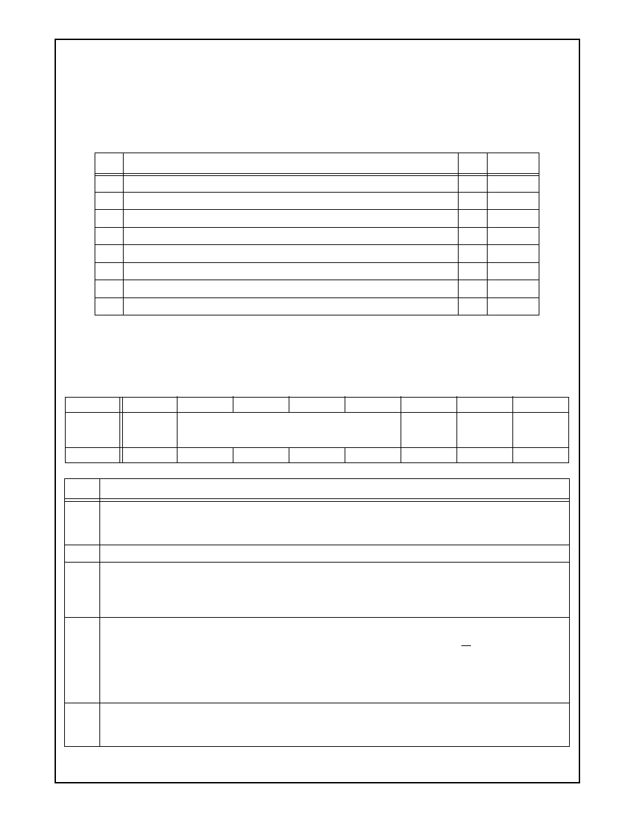
Table 22. Serial Port 1 Conguration Registers
2.14.2
Serial Port 1 Configuration Register
This register is reset by hardware to 02h.
Location:
Index F0h
Type:
R/W
Index
Conguration Register or Action
Type
Reset
30h Activate. See also bit 0 of the SIOCF1 register and bit 3 of the SIOCF6 register. R/W
00h
60h Base Address MSB register. Bits 7-3 (for A15-11) are read only, 00000b.
R/W
03h
61h Base Address LSB register. Bit 2-0 (for A2-0) are read only, 000b.
R/W
F8h
70h Interrupt Number and Wake-Up on IRQ Enable register
R/W
04h
71h Interrupt Type. Bit 1 is R/W; other bits are read only.
R/W
03h
74h Report no DMA Assignment
RO
04h
75h Report no DMA Assignment
RO
04h
F0h Serial Port 1 Conguration register
R/W
02h
Bit
76543210
Name
Bank
Select
Enable
Reserved
Busy
Indicator
Power
Mode
Control
TRI-STATE
Control
Reset
00000010
Bit
Description
7
Bank Select Enable. Enables bank switching for Serial Port 1.
0: Disabled (default).
1: Enabled
6-3
Reserved
2
Busy Indicator. This read only bit can be used by power management software to decide when to power-down
the Serial Port 1 logical device.
0: No transfer in progress (default).
1: Transfer in progress.
1
Power Mode Control. When the logical device is active in:
0: Low power mode
Serial Port 1 clock disabled. The output signals are set to their default states. The RI input signal can be
programmed to generate an interrupt. Registers are maintained (unlike Active bit in Index 30 that also
prevents access to Serial Port 1 registers).
1: Normal power mode
Serial Port 1 clock enabled. Serial Port 1 is functional when the logical device is active (default).
0
TRI-STATE Control. When enabled and the device is inactive, the logical device output pins are in TRI-STATE.
0: Disabled (default)
1: Enabled
相关PDF资料 |
PDF描述 |
|---|---|
| PC906N | 896 MHz - 940 MHz YAGI ANTENNA, 10.65 dBi GAIN, 65 deg 3dB BEAMWIDTH |
| PC926N | 928 MHz - 960 MHz YAGI ANTENNA, 10.65 dBi GAIN, 65 deg 3dB BEAMWIDTH |
| PCA.1D.694.CNAD42Z | CABLE TERMINATED, FEMALE, RF CONNECTOR, SOCKET |
| PCA.1D.694.CNAD42 | CABLE TERMINATED, FEMALE, RF CONNECTOR, SOCKET |
| PCA.1D.694.CNAD52Z | CABLE TERMINATED, FEMALE, RF CONNECTOR, SOCKET |
相关代理商/技术参数 |
参数描述 |
|---|---|
| PC87393VJG | 制造商:Texas Instruments 功能描述: 制造商:Texas Instruments 功能描述:IC, SUPER I/O DEVICE, TQFP-100, Logic Device Type:Buffer, Supply Voltage Min:3V, |
| PC87393-VJG | 制造商:NSC 制造商全称:National Semiconductor 功能描述:100-Pin LPC SuperI/O Devices for Portable Applications |
| PC87410 | 制造商:NSC 制造商全称:National Semiconductor 功能描述:PC87410 PCI-IDE Interface Controller |
| PC87410VLK | 制造商:Rochester Electronics LLC 功能描述:- Bulk |
| PC87413 | 制造商:NSC 制造商全称:National Semiconductor 功能描述:LPC ServerI/O for Servers and Workstations |
发布紧急采购,3分钟左右您将得到回复。