- 您现在的位置:买卖IC网 > PDF目录224693 > PC87393F-VJG (NATIONAL SEMICONDUCTOR CORP) 100-Pin LPC SuperI/O Devices for Portable Applications PDF资料下载
参数资料
| 型号: | PC87393F-VJG |
| 厂商: | NATIONAL SEMICONDUCTOR CORP |
| 元件分类: | 外设及接口 |
| 英文描述: | 100-Pin LPC SuperI/O Devices for Portable Applications |
| 中文描述: | MULTIFUNCTION PERIPHERAL, PQFP100 |
| 封装: | TQFP-100 |
| 文件页数: | 11/148页 |
| 文件大小: | 1733K |
| 代理商: | PC87393F-VJG |
第1页第2页第3页第4页第5页第6页第7页第8页第9页第10页当前第11页第12页第13页第14页第15页第16页第17页第18页第19页第20页第21页第22页第23页第24页第25页第26页第27页第28页第29页第30页第31页第32页第33页第34页第35页第36页第37页第38页第39页第40页第41页第42页第43页第44页第45页第46页第47页第48页第49页第50页第51页第52页第53页第54页第55页第56页第57页第58页第59页第60页第61页第62页第63页第64页第65页第66页第67页第68页第69页第70页第71页第72页第73页第74页第75页第76页第77页第78页第79页第80页第81页第82页第83页第84页第85页第86页第87页第88页第89页第90页第91页第92页第93页第94页第95页第96页第97页第98页第99页第100页第101页第102页第103页第104页第105页第106页第107页第108页第109页第110页第111页第112页第113页第114页第115页第116页第117页第118页第119页第120页第121页第122页第123页第124页第125页第126页第127页第128页第129页第130页第131页第132页第133页第134页第135页第136页第137页第138页第139页第140页第141页第142页第143页第144页第145页第146页第147页第148页
7.0 X-Bus Extension (Continued)
108
www.national.com
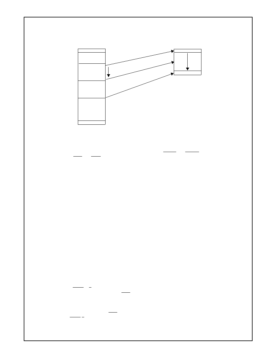
Figure 23. LPC to X-Bus Address Translation: Legacy and Extended Legacy BIOS Ranges
7.3.3
Extended Read/Write Signal Mode
This mode is essential for devices that have separate read and write signals for memory transactions and for I/O transac-
tions. While in this mode, the PC8739x routes I/O read and write signals to XIORD and XIOWR pins, and memory or FWH
read and write signals to XRD and XWR.
If the PC8739x is set to wake-up with the X-Bus signals configured to output pins (using strap pins XCNF2-0), the extended
mode is disabled, and must be re-enabled by the user.
7.3.4
Indirect Memory Read and Write Transaction
I/O mapped registers may be used through an LPC I/O transaction to perform an X-Bus memory transaction. This mecha-
nism uses the following X-Bus module registers:
q
Four Indirect Memory Address registers, XIMA3-XIMA0, representing address bits 31 to 0
q
One Indirect Memory Data register (XIMD), representing data bits 7 to 0
q
Two enable bits, one for each Select Conguration register, XZCNF0[5] and XZCNF1[5].
Following a write to the XIMD register, a memory write cycle appears on the X-Bus using the addresses and data from the
XIMA3-XIMA0 and XIMD registers. Following a read from the XIMD register, a memory read cycle appears on the X-Bus
using the addresses from these same registers. The returned data from the X-Bus cycle is used to finish the LPC I/O read
cycle from XIMD register.
The read or write cycles appear only if one of the Indirect Memory Cycle Enable bits (XZCNF0[5] or XZCNF1[5]) is set. If
both of these bits are set, select 1 is ignored and the transaction takes place according to select 0 settings. All X-Bus cycle
configurations are the same as defined in the X-Bus Select Configuration registers (XZCNF0 and XZCNF1).
7.3.5
Normal Address Mode X-Bus Transactions
The read and write transactions in Normal address mode are similar to those used in the X-Bus or ISA bus. At least two idle
cycles are inserted at the end of each X-Bus transaction cycle (there may be more idle cycles due to the LPC transactions).
Once a read cycle on the LPC falls within the range of any of the enabled decoded address ranges of the X-Bus functional
block, a read cycle begins. A read cycle (Figure 24) starts by outputting the address signals on address signals XA19-0 on
the rising edge of the clock. During this time, the PC8739x does not drive the data bus signals XD7-0. One LPC clock cycle
later, a chip select signal XCS1 or 0 is asserted, based on the address accessed and the select signal mapping. Three clock
cycles later, on the next rising edge of the clock, the XRD signal is asserted (set to 0) indicating that this is a read cycle and
enabling the device being accessed to drive the data bus within 16 clock cycles plus the internally programmed wait state
period. If XRDY use is enabled for this zone, XRDY input value is then checked on the rising edge of the clock, and the trans-
action is extended until XRDY is detected to be high. Four clock cycles later, the input data XD7-0 is sampled on the rising
edge of the clock. One LPC clock cycle later, XRD is de-asserted (set to 1) and one clock cycle later, the transaction is com-
pleted by de-asserting XCS1-0. The address is retained for the duration of two more cycles, after which the address lines
change their values to 0.
LPC Bus Address
FFFFFFFFh
xFFFFFFFh
X-Bus Address
000FFFFFh
xFFE0000h
00000000h
**
*
000F0000h
000EFFFFh
000E0000h
Legacy BIOS
Extended
Legacy BIOS
相关PDF资料 |
PDF描述 |
|---|---|
| PC906N | 896 MHz - 940 MHz YAGI ANTENNA, 10.65 dBi GAIN, 65 deg 3dB BEAMWIDTH |
| PC926N | 928 MHz - 960 MHz YAGI ANTENNA, 10.65 dBi GAIN, 65 deg 3dB BEAMWIDTH |
| PCA.1D.694.CNAD42Z | CABLE TERMINATED, FEMALE, RF CONNECTOR, SOCKET |
| PCA.1D.694.CNAD42 | CABLE TERMINATED, FEMALE, RF CONNECTOR, SOCKET |
| PCA.1D.694.CNAD52Z | CABLE TERMINATED, FEMALE, RF CONNECTOR, SOCKET |
相关代理商/技术参数 |
参数描述 |
|---|---|
| PC87393VJG | 制造商:Texas Instruments 功能描述: 制造商:Texas Instruments 功能描述:IC, SUPER I/O DEVICE, TQFP-100, Logic Device Type:Buffer, Supply Voltage Min:3V, |
| PC87393-VJG | 制造商:NSC 制造商全称:National Semiconductor 功能描述:100-Pin LPC SuperI/O Devices for Portable Applications |
| PC87410 | 制造商:NSC 制造商全称:National Semiconductor 功能描述:PC87410 PCI-IDE Interface Controller |
| PC87410VLK | 制造商:Rochester Electronics LLC 功能描述:- Bulk |
| PC87413 | 制造商:NSC 制造商全称:National Semiconductor 功能描述:LPC ServerI/O for Servers and Workstations |
发布紧急采购,3分钟左右您将得到回复。