- 您现在的位置:买卖IC网 > PDF目录68559 > W9725G8JB-25I (WINBOND ELECTRONICS CORP) DDR DRAM, PBGA84 PDF资料下载
参数资料
| 型号: | W9725G8JB-25I |
| 厂商: | WINBOND ELECTRONICS CORP |
| 元件分类: | DRAM |
| 英文描述: | DDR DRAM, PBGA84 |
| 封装: | 8 X 12.50 MM, ROHS COMPLIANT, WBGA-84 |
| 文件页数: | 13/86页 |
| 文件大小: | 1462K |
| 代理商: | W9725G8JB-25I |
第1页第2页第3页第4页第5页第6页第7页第8页第9页第10页第11页第12页当前第13页第14页第15页第16页第17页第18页第19页第20页第21页第22页第23页第24页第25页第26页第27页第28页第29页第30页第31页第32页第33页第34页第35页第36页第37页第38页第39页第40页第41页第42页第43页第44页第45页第46页第47页第48页第49页第50页第51页第52页第53页第54页第55页第56页第57页第58页第59页第60页第61页第62页第63页第64页第65页第66页第67页第68页第69页第70页第71页第72页第73页第74页第75页第76页第77页第78页第79页第80页第81页第82页第83页第84页第85页第86页
W9725G8JB
Publication Release Date: Oct. 12, 2010
- 20 -
Revision A01
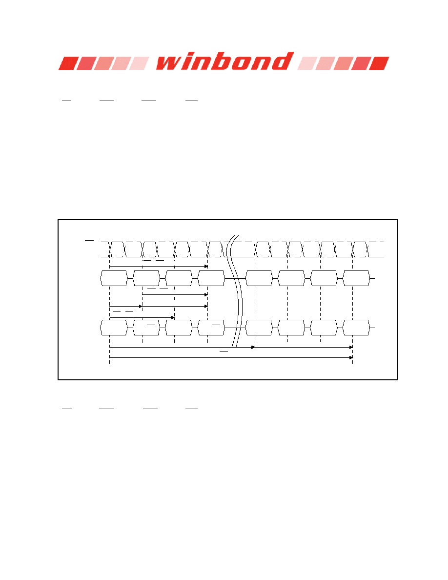
7.3
Command Function
7.3.1
Bank Activate Command
( CS = "L", RAS = "L", CAS = "H", WE = "H", BA0, BA1 = Bank, A0 to A12 be row address)
The Bank Activate command must be applied before any Read or Write operation can be executed.
Immediately after the bank active command, the DDR2 SDRAM can accept a read or write command
on the following clock cycle. If a Read/Write command is issued to a bank that has not satisfied the
tRCDmin specification, then additive latency must be programmed into the device to delay when the
Read/Write command is internally issued to the device. The additive latency value must be chosen to
assure tRCDmin is satisfied. Additive latencies of 0, 1, 2, 3, 4, 5 and 6 are supported. Once a bank has
been activated it must be precharged before another Bank Activate command can be applied to the
same bank. The bank active and precharge times are defined as tRAS and tRP, respectively. The
minimum time interval between successive Bank Activate commands to the same bank is determined
by the RAS cycle time of the device (tRC). The minimum time interval between Bank Activate
commands is tRRD.
T0
T1
T2
T3
Tn
Tn+1
Tn+2
Tn+3
Bank A
Row Addr.
Bank A
Col. Addr.
Bank B
Row Addr.
Bank B
Col. Addr.
Bank A
Addr.
Bank B
Addr.
Bank A
Row Addr.
CAS - CAS delay time(tCCD)
tRCD = 1
Additive Latency delay(AL)
Read Begins
Bank A
Activate
Bank A
Post CAS
Read
Bank B
Activate
Bank B
Post CAS
Read
Bank A
Precharge
Bank B
Precharge
Bank A
Activate
Bank Active (
≥ tRAS)
RAS Cycle time (
≥ tRC)
Bank Precharge time (
≥ tRP)
Command
Address
RAS - RAS delay time(
≥ tRRD)
CLK
Internal RAS - RAS delay (
≥ tRCDmin)
Figure 12
– Bank activate command cycle: tRCD = 3, AL = 2, tRP = 3, tRRD = 2, tCCD = 2
7.3.2
Read Command
(
CS = "L", RAS = "H", CAS = "L", WE = "H", BA0, BA1 = Bank, A10 = "L", A0 to A9 = Column
Address)
The READ command is used to initiate a burst read access to an active row. The value on BA0, BA1
inputs selects the bank, and the A0 to A9 address inputs determine the starting column address. The
address input A10 determines whether or not Auto-precharge is used. If Auto-precharge is selected,
the row being accessed will be precharged at the end of the READ burst; if Auto-precharge is not
selected, the row will remain open for subsequent accesses.
相关PDF资料 |
PDF描述 |
|---|---|
| W972GG8JB-25I | 256M X 8 DDR DRAM, 0.4 ns, PBGA60 |
| W972GG8JB-18 | 256M X 8 DDR DRAM, 0.35 ns, PBGA60 |
| W9751G6JB-18 | 32M X 16 DDR DRAM, 0.35 ns, PBGA84 |
| W981204AH-8H | 32M X 4 SYNCHRONOUS DRAM, 6 ns, PDSO54 |
| W981216BH75L | 8M X 16 SYNCHRONOUS DRAM, 5.4 ns, PDSO54 |
相关代理商/技术参数 |
参数描述 |
|---|---|
| W9725G8JB25ITR | 制造商:Winbond Electronics Corp 功能描述:256M DDR2-800, X8, IND TEMP |
| W9725G8JB25TR | 制造商:Winbond Electronics Corp 功能描述:256M DDR2-800, X8 |
| W9725G8KB-18 | 制造商:Winbond Electronics 功能描述:IC MEMORY 制造商:Winbond Electronics Corp 功能描述:IC MEMORY |
| W9725G8KB-25 | 制造商:Winbond Electronics 功能描述:IC MEMORY 制造商:Winbond Electronics Corp 功能描述:IC MEMORY |
| W9725G8KB-25 TR | 制造商:Winbond Electronics Corp 功能描述:256M DDR2-800, X8 |
发布紧急采购,3分钟左右您将得到回复。