- 您现在的位置:买卖IC网 > PDF目录68559 > W9725G8JB-25I (WINBOND ELECTRONICS CORP) DDR DRAM, PBGA84 PDF资料下载
参数资料
| 型号: | W9725G8JB-25I |
| 厂商: | WINBOND ELECTRONICS CORP |
| 元件分类: | DRAM |
| 英文描述: | DDR DRAM, PBGA84 |
| 封装: | 8 X 12.50 MM, ROHS COMPLIANT, WBGA-84 |
| 文件页数: | 62/86页 |
| 文件大小: | 1462K |
| 代理商: | W9725G8JB-25I |
第1页第2页第3页第4页第5页第6页第7页第8页第9页第10页第11页第12页第13页第14页第15页第16页第17页第18页第19页第20页第21页第22页第23页第24页第25页第26页第27页第28页第29页第30页第31页第32页第33页第34页第35页第36页第37页第38页第39页第40页第41页第42页第43页第44页第45页第46页第47页第48页第49页第50页第51页第52页第53页第54页第55页第56页第57页第58页第59页第60页第61页当前第62页第63页第64页第65页第66页第67页第68页第69页第70页第71页第72页第73页第74页第75页第76页第77页第78页第79页第80页第81页第82页第83页第84页第85页第86页
W9725G8JB
Publication Release Date: Oct. 12, 2010
- 65 -
Revision A01
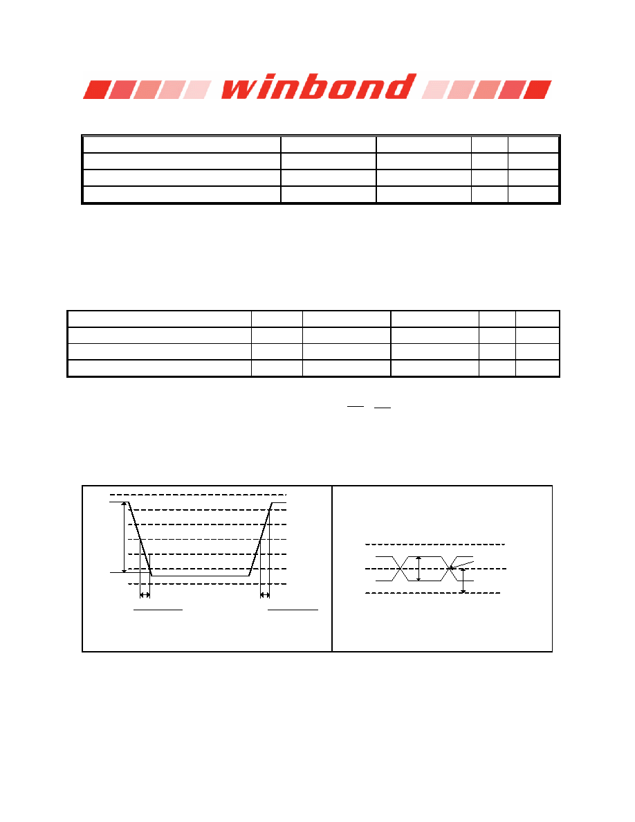
9.12 AC Input Test Conditions
(0°C
≤ TCASE ≤ 85°C for -18/-25/-3, -40°C ≤ TCASE ≤ 95°C for 25I, VDD, VDDQ = 1.8V ± 0.1V)
CONDITION
SYMBOL
VALUE
UNIT
NOTES
Input reference voltage
VREF
0.5 x VDDQ
V
1
Input signal maximum peak to peak swing
VSWING(MAX)
1.0
V
1
Input signal minimum slew rate
SLEW
1.0
V/nS
2, 3
Notes:
1. Input waveform timing is referenced to the input signal crossing through the VIH/IL(ac) level applied to the device under test.
2. The input signal minimum slew rate is to be maintained over the range from VREF to VIH(ac) min for rising edges and the
range from VREF to VIL(ac) max for falling edges as shown in the below figure.
3. AC timings are referenced with input waveforms switching from VIL(ac) to VIH(ac) on the positive transitions and VIH(ac) to
VIL(ac) on the negative transitions.
9.13 Differential Input/Output AC Logic Levels
(0°C
≤ TCASE ≤ 85°C for -18/-25/-3, -40°C ≤ TCASE ≤ 95°C for 25I, VDD, VDDQ = 1.8V ± 0.1V)
PARAMETER
SYM.
MIN.
MAX.
UNIT
NOTES
AC differential input voltage
VID (ac)
0.5
VDDQ + 0.6
V
1
AC differential cross point input voltage
VIX (ac)
0.5 x VDDQ - 0.175
0.5 x VDDQ + 0.175
V
2
AC differential cross point output voltage
VOX (ac)
0.5 x VDDQ - 0.125
0.5 x VDDQ + 0.125
V
3
Notes:
1. VID (ac) specifies the input differential voltage |VTR -VCP | required for switching, where VTR is the true input signal (such
as CLK, DQS) and VCP is the complementary input signal (such as CLK , DQS ). The minimum value is equal to VIH (ac) -
VIL (ac).
2. The typical value of VIX (ac) is expected to be about 0.5 x VDDQ of the transmitting device and VIX (ac) is expected to track
variations in VDDQ. VIX (ac) indicates the voltage at which differential input signals must cross.
3. The typical value of VOX (ac) is expected to be about 0.5 x VDDQ of the transmitting device and VOX (ac) is expected to
track variations in VDDQ. VOX (ac) indicates the voltage at which differential output signals must cross.
ΔTF
ΔTR
VDDQ
VIH(ac) min
Falling Slew =
Rising Slew =
VIH(dc) min
VREF
VIL(dc) max
VIL(ac) max
VSS
VSWING(MAX)
VREF - VIL(ac) max
ΔTF
VIH(ac) min - VREF
ΔTR
VDDQ
VSSQ
VIX or VOX
VID
VTR
Crossing point
VCP
Figure 28
– AC input test signal and Differential signal levels waveform
相关PDF资料 |
PDF描述 |
|---|---|
| W972GG8JB-25I | 256M X 8 DDR DRAM, 0.4 ns, PBGA60 |
| W972GG8JB-18 | 256M X 8 DDR DRAM, 0.35 ns, PBGA60 |
| W9751G6JB-18 | 32M X 16 DDR DRAM, 0.35 ns, PBGA84 |
| W981204AH-8H | 32M X 4 SYNCHRONOUS DRAM, 6 ns, PDSO54 |
| W981216BH75L | 8M X 16 SYNCHRONOUS DRAM, 5.4 ns, PDSO54 |
相关代理商/技术参数 |
参数描述 |
|---|---|
| W9725G8JB25ITR | 制造商:Winbond Electronics Corp 功能描述:256M DDR2-800, X8, IND TEMP |
| W9725G8JB25TR | 制造商:Winbond Electronics Corp 功能描述:256M DDR2-800, X8 |
| W9725G8KB-18 | 制造商:Winbond Electronics 功能描述:IC MEMORY 制造商:Winbond Electronics Corp 功能描述:IC MEMORY |
| W9725G8KB-25 | 制造商:Winbond Electronics 功能描述:IC MEMORY 制造商:Winbond Electronics Corp 功能描述:IC MEMORY |
| W9725G8KB-25 TR | 制造商:Winbond Electronics Corp 功能描述:256M DDR2-800, X8 |
发布紧急采购,3分钟左右您将得到回复。