- 您现在的位置:买卖IC网 > PDF目录68559 > W9725G8JB-25I (WINBOND ELECTRONICS CORP) DDR DRAM, PBGA84 PDF资料下载
参数资料
| 型号: | W9725G8JB-25I |
| 厂商: | WINBOND ELECTRONICS CORP |
| 元件分类: | DRAM |
| 英文描述: | DDR DRAM, PBGA84 |
| 封装: | 8 X 12.50 MM, ROHS COMPLIANT, WBGA-84 |
| 文件页数: | 43/86页 |
| 文件大小: | 1462K |
| 代理商: | W9725G8JB-25I |
第1页第2页第3页第4页第5页第6页第7页第8页第9页第10页第11页第12页第13页第14页第15页第16页第17页第18页第19页第20页第21页第22页第23页第24页第25页第26页第27页第28页第29页第30页第31页第32页第33页第34页第35页第36页第37页第38页第39页第40页第41页第42页当前第43页第44页第45页第46页第47页第48页第49页第50页第51页第52页第53页第54页第55页第56页第57页第58页第59页第60页第61页第62页第63页第64页第65页第66页第67页第68页第69页第70页第71页第72页第73页第74页第75页第76页第77页第78页第79页第80页第81页第82页第83页第84页第85页第86页
W9725G8JB
Publication Release Date: Oct. 12, 2010
- 48 -
Revision A01
11. There are two sets of values listed for Command/Address input hold time: tIH(base) and tIH(ref). The tIH(ref) value (for
reference only) is equivalent to the baseline value of tIH(base) at VREF when the slew rate is 1.0 V/nS. The baseline value
tIH(base) is the JEDEC defined value, referenced from the input signal crossing at the VIL(dc) level for a rising signal and
VIH(dc) for a falling signal applied to the device under test. See Figure 17. If the Command/Address slew rate is not equal to
1.0 V/nS, then the baseline values must be derated by adding the values from table tIS/tIH derating values for DDR2-667,
DDR2-800 and DDR2-1066 (page 55).
12. The maximum limit for the tWPST parameter is not a device limit. The device operates with a greater value for this
parameter, but system performance (bus turnaround) will degrades accordingly.
13. tDQSQ: Consists of data pin skew and output pattern effects, and p-channel to n-channel variation of the output drivers as
well as output Slew Rate mismatch between DQS / DQS and associated DQ in any given cycle.
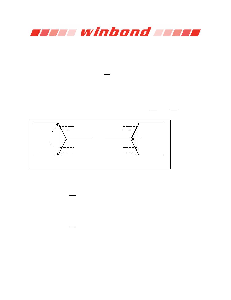
14. tRPST end point and tRPRE begin point are not referenced to a specific voltage level but specify when the device output is
no longer driving (tRPST), or begins driving (tRPRE). Figure 18 shows a method to calculate these points when the device
is no longer driving (tRPST), or begins driving (tRPRE) by measuring the signal at two different voltages. The actual voltage
measurement points are not critical as long as the calculation is consistent.
15. tHZ and tLZ transitions occur in the same access time as valid data transitions. These parameters are referenced to a
specific voltage level which specifies when the device output is no longer driving (tHZ), or begins driving (tLZ). Figure 18
shows a method to calculate the point when device is no longer driving (tHZ), or begins driving (tLZ) by measuring the
signal at two different voltages. The actual voltage measurement points are not critical as long as the calculation is
consistent. tLZ(DQ) refers to tLZ of
the DQs and tLZ(DQS) refers to tLZ of the (DQS, DQS , RDQS, RDQS ) each treated
as single-ended signal.
VOH - x mV
VTT - 2x mV
VTT - x mV
VOH - 2x mV
VOL + 2x mV
VOL + x mV
VTT + x mV
VTT + 2x mV
tRPST end point
tRPRE begin point
tHZ,tRPST end point = 2 x T1 - T2
tLZ,tRPRE begin point = 2 x T1 - T2
tHZ
T1 T2
tLZ
T1 T2
Figure 18
– Method for calculating transitions and endpoints
16. Input waveform timing tDS with differential data strobe enabled MR[bit10]=0. There are two sets of values listed for DQ and
DM input setup time: tDS(base) and tDS(ref). The tDS(ref) value (for reference only) is equivalent to the baseline value
tDS(base) at VREF when the slew rate is 2.0 V/nS, differentially. The baseline value tDS(base) is the JEDEC defined value,
referenced from the input signal crossing at the VIH(ac) level to the differential data strobe crosspoint for a rising signal, and
from the input signal crossing at the VIL(ac) level to the differential data strobe crosspoint for a falling signal applied to the
device under test. DQS, DQS signals must be monotonic between VIL(dc)max and VIH(dc)min. See Figure 19. If the
differential DQS slew rate is not equal to 2.0 V/nS, then the baseline values must be derated by adding the values from
table of DDR2-667, DDR2-800 and DDR2-1066 tDS/tDH derating with differential data strobe (page 60).
17. Input waveform timing tDH with differential data strobe enabled MR[bit10]=0. There are two sets of values listed for DQ and
DM input hold time: tDH(base) and tDH(ref). The tDH(ref) value (for reference only) is equivalent to the baseline value
tDH(base) at VREF when the slew rate is 2.0 V/nS, differentially. The baseline value tDH(base) is the JEDEC defined value,
referenced from the differential data strobe crosspoint to the input signal crossing at the VIH(dc) level for a falling signal and
from the differential data strobe crosspoint to the input signal crossing at the VIL(dc) level for a rising signal applied to the
device under test. DQS, DQS signals must be monotonic between VIL(dc)max and VIH(dc)min. See Figure 19. If the
differential DQS slew rate is not equal to 2.0 V/nS, then the baseline values must be derated by adding the values from
table of DDR2-667, DDR2-800 and DDR2-1066 tDS/tDH derating with differential data strobe (page 60).
相关PDF资料 |
PDF描述 |
|---|---|
| W972GG8JB-25I | 256M X 8 DDR DRAM, 0.4 ns, PBGA60 |
| W972GG8JB-18 | 256M X 8 DDR DRAM, 0.35 ns, PBGA60 |
| W9751G6JB-18 | 32M X 16 DDR DRAM, 0.35 ns, PBGA84 |
| W981204AH-8H | 32M X 4 SYNCHRONOUS DRAM, 6 ns, PDSO54 |
| W981216BH75L | 8M X 16 SYNCHRONOUS DRAM, 5.4 ns, PDSO54 |
相关代理商/技术参数 |
参数描述 |
|---|---|
| W9725G8JB25ITR | 制造商:Winbond Electronics Corp 功能描述:256M DDR2-800, X8, IND TEMP |
| W9725G8JB25TR | 制造商:Winbond Electronics Corp 功能描述:256M DDR2-800, X8 |
| W9725G8KB-18 | 制造商:Winbond Electronics 功能描述:IC MEMORY 制造商:Winbond Electronics Corp 功能描述:IC MEMORY |
| W9725G8KB-25 | 制造商:Winbond Electronics 功能描述:IC MEMORY 制造商:Winbond Electronics Corp 功能描述:IC MEMORY |
| W9725G8KB-25 TR | 制造商:Winbond Electronics Corp 功能描述:256M DDR2-800, X8 |
发布紧急采购,3分钟左右您将得到回复。