- 您现在的位置:买卖IC网 > PDF目录68559 > W9725G8JB-25I (WINBOND ELECTRONICS CORP) DDR DRAM, PBGA84 PDF资料下载
参数资料
| 型号: | W9725G8JB-25I |
| 厂商: | WINBOND ELECTRONICS CORP |
| 元件分类: | DRAM |
| 英文描述: | DDR DRAM, PBGA84 |
| 封装: | 8 X 12.50 MM, ROHS COMPLIANT, WBGA-84 |
| 文件页数: | 44/86页 |
| 文件大小: | 1462K |
| 代理商: | W9725G8JB-25I |
第1页第2页第3页第4页第5页第6页第7页第8页第9页第10页第11页第12页第13页第14页第15页第16页第17页第18页第19页第20页第21页第22页第23页第24页第25页第26页第27页第28页第29页第30页第31页第32页第33页第34页第35页第36页第37页第38页第39页第40页第41页第42页第43页当前第44页第45页第46页第47页第48页第49页第50页第51页第52页第53页第54页第55页第56页第57页第58页第59页第60页第61页第62页第63页第64页第65页第66页第67页第68页第69页第70页第71页第72页第73页第74页第75页第76页第77页第78页第79页第80页第81页第82页第83页第84页第85页第86页
W9725G8JB
Publication Release Date: Oct. 12, 2010
- 49 -
Revision A01
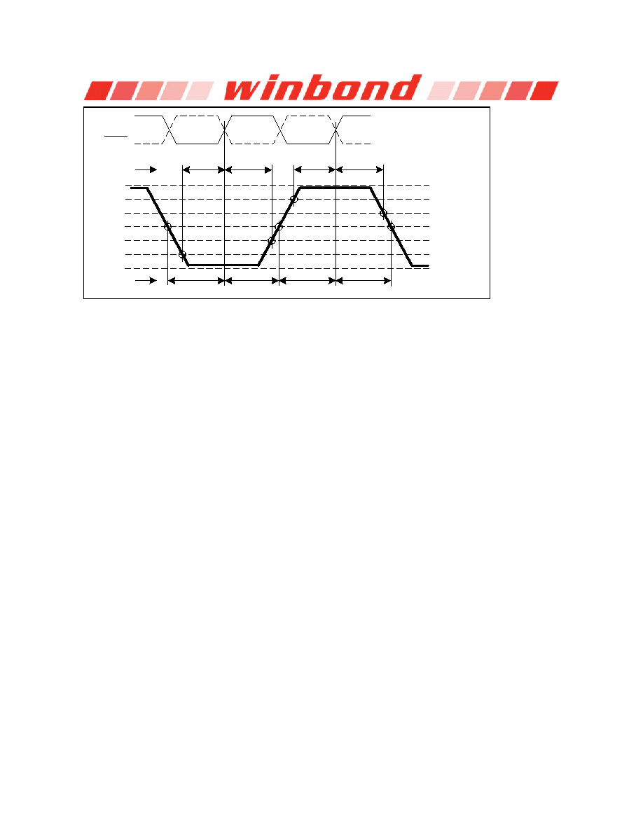
DQS
tDS(base) tDH(base)
VDDQ
VIH(ac) min
VIH(dc) min
VREF(dc)
VIL(dc) max
VIL(ac) max
VSS
tDS(ref)
tDH(ref)
tDS(ref)
tDH(ref)
Logic levels
VREF levels
Figure 19
– Differential input waveform timing – tDS and tDH
18. User can choose which active power down exit timing to use via MRS (bit 12). tXARD is expected to be used for fast active
power down exit timing. tXARDS is expected to be used for slow active power down exit timing.
19. AL = Additive Latency.
20. ODT turn on time min is when the device leaves high impedance and ODT resistance begins to turn on. ODT turn on time
max is when the ODT resistance is fully on. Both are measure from tAOND, which is interpreted differently per speed bin.
For DDR2-667/800/1066, tAOND is 2 clock cycles after the clock edge that registered a first ODT HIGH counting the actual
input clock edges.
21. ODT turn off time min is when the device starts to turn off ODT resistance. ODT turn off time max is when the bus is in high
impedance. Both are measured from tAOFD.
For DDR2-667/800: This is interpreted differently per speed bin. If tCK(avg) = 3 nS is assumed, tAOFD is 1.5 nS (=
0.5 x 3 nS) after the second trailing clock edge counting from the clock edge that registered a first ODT LOW and by
counting the actual input clock edges.
For DDR2-1066: This is interpreted as 0.5 x tCK(avg) [nS] after the second trailing clock edge counting from the
clock edge that registered a first ODT LOW and by counting the actual input clock edges. tAOFD is 0.9375 [nS] (=
0.5 x 1.875 [nS]) after the second trailing clock edge counting from the clock edge that registered a first ODT LOW
and by counting the actual input clock edges.
22. The clock frequency is allowed to change during Self Refresh mode or precharge power-down mode. In case of clock
frequency change during precharge power-down, a specific procedure is required as described in section 7.10.
23. For these parameters, the DDR2 SDRAM device is characterized and verified to support tnPARAM = RU{tPARAM /
tCK(avg)}, which is in clock cycles, assuming all input clock jitter specifications are satisfied.
Examples:
The device will support tnRP = RU{tRP / tCK(avg)}, which is in clock cycles, if all input clock jitter specifications are
met. This means: For DDR2-667 5-5-5, of which tRP = 15nS, the device will support tnRP = RU{tRP / tCK(avg)} = 5,
i.e. as long as the input clock jitter specifications are met, Precharge command at Tm and Active command at Tm+5
is valid even if (Tm+5 - Tm) is less than 15nS due to input clock jitter. For DDR2-1066 7-7-7, of which tRP = 13.125
nS, the device will support tnRP = RU{tRP / tCK(avg)} = 7, i.e. as long as the input clock jitter specifications are met,
Precharge command at Tm and Active command at Tm+7 is valid even if (Tm+7 - Tm) is less than 13.125 nS due to
input clock jitter.
24. tDAL [nCK] = WR [nCK] + tnRP [nCK] = WR + RU {tRP [pS] / tCK(avg) [pS] }, where WR is the value programmed in the
mode register set and RU stands for round up.
Example:
For DDR2-1066 7-7-7 at tCK(avg) = 1.875 nS with WR programmed to 8 nCK, tDAL = 8 + RU{13.125 nS / 1.875
nS} [nCK] = 8 + 7 [nCK] = 15 [nCK].
相关PDF资料 |
PDF描述 |
|---|---|
| W972GG8JB-25I | 256M X 8 DDR DRAM, 0.4 ns, PBGA60 |
| W972GG8JB-18 | 256M X 8 DDR DRAM, 0.35 ns, PBGA60 |
| W9751G6JB-18 | 32M X 16 DDR DRAM, 0.35 ns, PBGA84 |
| W981204AH-8H | 32M X 4 SYNCHRONOUS DRAM, 6 ns, PDSO54 |
| W981216BH75L | 8M X 16 SYNCHRONOUS DRAM, 5.4 ns, PDSO54 |
相关代理商/技术参数 |
参数描述 |
|---|---|
| W9725G8JB25ITR | 制造商:Winbond Electronics Corp 功能描述:256M DDR2-800, X8, IND TEMP |
| W9725G8JB25TR | 制造商:Winbond Electronics Corp 功能描述:256M DDR2-800, X8 |
| W9725G8KB-18 | 制造商:Winbond Electronics 功能描述:IC MEMORY 制造商:Winbond Electronics Corp 功能描述:IC MEMORY |
| W9725G8KB-25 | 制造商:Winbond Electronics 功能描述:IC MEMORY 制造商:Winbond Electronics Corp 功能描述:IC MEMORY |
| W9725G8KB-25 TR | 制造商:Winbond Electronics Corp 功能描述:256M DDR2-800, X8 |
发布紧急采购,3分钟左右您将得到回复。