- 您现在的位置:买卖IC网 > PDF目录68559 > W9725G8JB-25I (WINBOND ELECTRONICS CORP) DDR DRAM, PBGA84 PDF资料下载
参数资料
| 型号: | W9725G8JB-25I |
| 厂商: | WINBOND ELECTRONICS CORP |
| 元件分类: | DRAM |
| 英文描述: | DDR DRAM, PBGA84 |
| 封装: | 8 X 12.50 MM, ROHS COMPLIANT, WBGA-84 |
| 文件页数: | 3/86页 |
| 文件大小: | 1462K |
| 代理商: | W9725G8JB-25I |
第1页第2页当前第3页第4页第5页第6页第7页第8页第9页第10页第11页第12页第13页第14页第15页第16页第17页第18页第19页第20页第21页第22页第23页第24页第25页第26页第27页第28页第29页第30页第31页第32页第33页第34页第35页第36页第37页第38页第39页第40页第41页第42页第43页第44页第45页第46页第47页第48页第49页第50页第51页第52页第53页第54页第55页第56页第57页第58页第59页第60页第61页第62页第63页第64页第65页第66页第67页第68页第69页第70页第71页第72页第73页第74页第75页第76页第77页第78页第79页第80页第81页第82页第83页第84页第85页第86页
W9725G8JB
Publication Release Date: Oct. 12, 2010
- 11 -
Revision A01
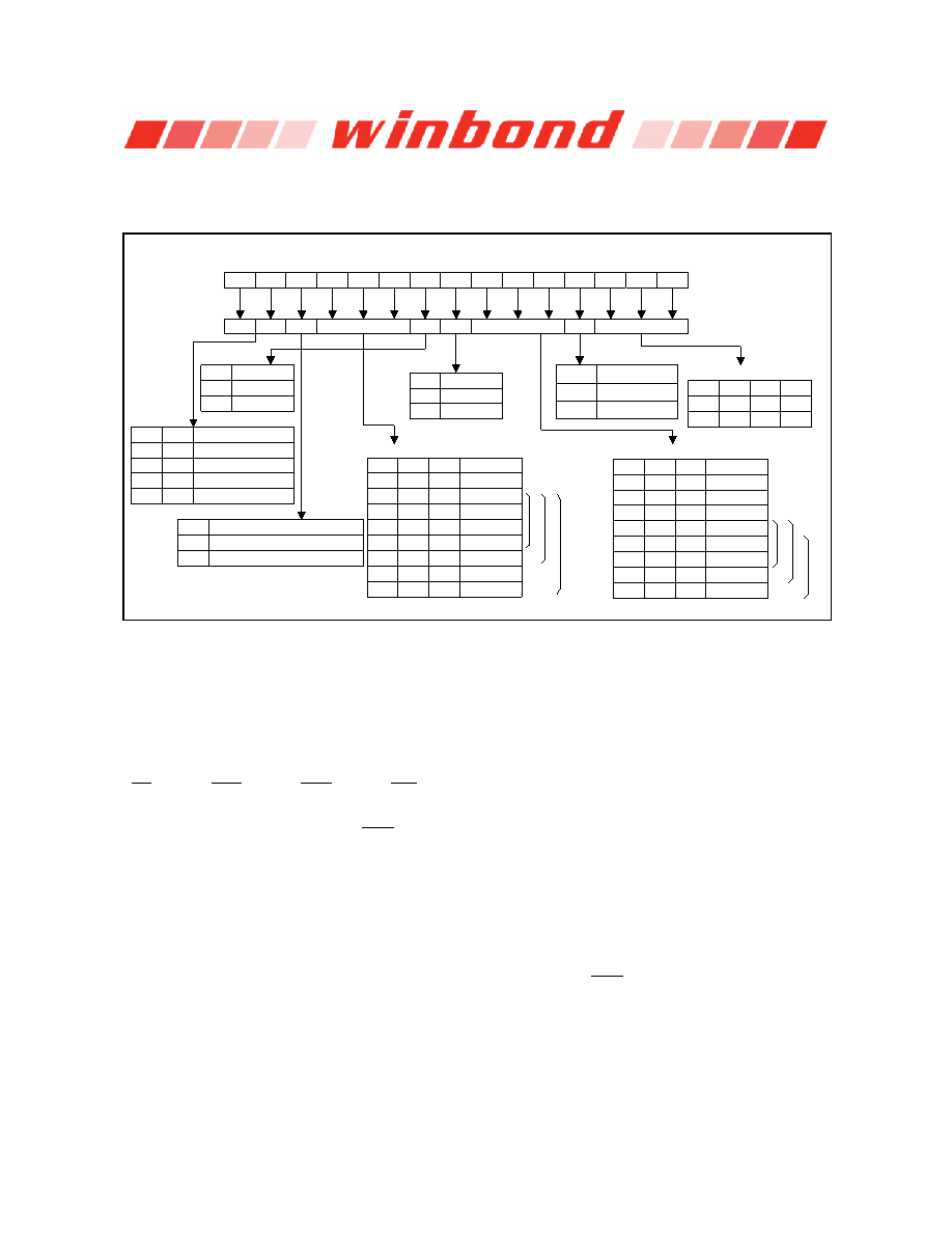
SDRAM. Burst address sequence type is defined by A3, CAS Latency is defined by A[6:4]. The DDR2
does not support half clock latency mode. A7 is used for test mode. A8 is used for DLL reset. A7 must
be set to LOW for normal MRS operation. Write recovery time WR is defined by A[11:9]. Refer to the
table for specific codes.
BA0
A12
A11
A10
A9
A8
A7
A6
A5
A4
A3
A2
A1
A0
PD
WR
DLL
BT
CAS Latency
Burst Length
TM
A8
0
1
DLL Reset
No
Yes
BA1
BA0
0
1
0
1
MRS mode
MR
EMR (1)
EMR (2)
EMR (3)
A12
1
0
Active power down exit time
Fast exit (use tXARD)
Slow exit (use tXARDS)
Burst Length
Address Field
Mode Register
Write recovery for Auto-precharge
CAS Latency
A6
0
1
A5
0
1
0
1
A4
0
1
0
1
0
1
0
Latency
Reserved
3
4
5
7
6
Reserved
A2
0
A1
1
A0
0
1
BL
4
8
A11
0
1
A10
0
1
0
1
A9
0
1
0
1
0
1
0
WR *
Reserved
2
3
4
5
6
8
7
A7
0
1
Mode
Normal
Test
A3
0
1
Burst Type
Sequential
Interleave
0
D
R
2
-6
6
7
D
R
2
-8
0
D
R
2
-1
0
6
D
R
2
-8
0
D
R
2
-1
0
6
D
R
2
-6
6
7
BA1
0
Note:
1. WR (write recovery for Auto-precharge) min is determined by tCK(avg) max and WR max is determined by tCK(avg) min.
WR[cycles] = RU{ tWR[nS] / tCK(avg)[nS] }, where RU stands for round up. The mode register must be programmed to this
value. This is also used with tRP to determine tDAL.
Figure 2
– Mode Register Set (MRS)
7.2.2
Extend Mode Register Set Commands (EMRS)
7.2.2.1
Extend Mode Register Set Command (1), EMR (1)
( CS = "L", RAS = "L", CAS = "L", WE = "L", BA0 = "H", BA1 = "L, A0 to A12 = Register data)
The extended mode register (1) stores the data for enabling or disabling the DLL, output driver
strength, additive latency, ODT, DQS disable, OCD program. The default value of the extended
mode register (1) is not defined, therefore the extended mode register (1) must be programmed during
initialization for proper operation. The DDR2 SDRAM should be in all bank precharge with CKE
already high prior to writing into the extended mode register (1). The mode register set command
cycle time (tMRD) must be satisfied to complete the write operation to the extended mode register (1).
Extended mode register (1) contents can be changed using the same command and clock cycle
requirements during normal operation as long as all banks are in the precharge state. A0 is used for
DLL enable or disable. A1 is used for enabling a reduced strength output driver. A[5:3] determines the
additive latency, A[9:7] are used for OCD control, A10 is used for
DQS disable and A11 is used for
RDQS enable. A2 and A6 are used for ODT setting.
相关PDF资料 |
PDF描述 |
|---|---|
| W972GG8JB-25I | 256M X 8 DDR DRAM, 0.4 ns, PBGA60 |
| W972GG8JB-18 | 256M X 8 DDR DRAM, 0.35 ns, PBGA60 |
| W9751G6JB-18 | 32M X 16 DDR DRAM, 0.35 ns, PBGA84 |
| W981204AH-8H | 32M X 4 SYNCHRONOUS DRAM, 6 ns, PDSO54 |
| W981216BH75L | 8M X 16 SYNCHRONOUS DRAM, 5.4 ns, PDSO54 |
相关代理商/技术参数 |
参数描述 |
|---|---|
| W9725G8JB25ITR | 制造商:Winbond Electronics Corp 功能描述:256M DDR2-800, X8, IND TEMP |
| W9725G8JB25TR | 制造商:Winbond Electronics Corp 功能描述:256M DDR2-800, X8 |
| W9725G8KB-18 | 制造商:Winbond Electronics 功能描述:IC MEMORY 制造商:Winbond Electronics Corp 功能描述:IC MEMORY |
| W9725G8KB-25 | 制造商:Winbond Electronics 功能描述:IC MEMORY 制造商:Winbond Electronics Corp 功能描述:IC MEMORY |
| W9725G8KB-25 TR | 制造商:Winbond Electronics Corp 功能描述:256M DDR2-800, X8 |
发布紧急采购,3分钟左右您将得到回复。