- 您现在的位置:买卖IC网 > PDF目录68559 > W9725G8JB-25I (WINBOND ELECTRONICS CORP) DDR DRAM, PBGA84 PDF资料下载
参数资料
| 型号: | W9725G8JB-25I |
| 厂商: | WINBOND ELECTRONICS CORP |
| 元件分类: | DRAM |
| 英文描述: | DDR DRAM, PBGA84 |
| 封装: | 8 X 12.50 MM, ROHS COMPLIANT, WBGA-84 |
| 文件页数: | 40/86页 |
| 文件大小: | 1462K |
| 代理商: | W9725G8JB-25I |
第1页第2页第3页第4页第5页第6页第7页第8页第9页第10页第11页第12页第13页第14页第15页第16页第17页第18页第19页第20页第21页第22页第23页第24页第25页第26页第27页第28页第29页第30页第31页第32页第33页第34页第35页第36页第37页第38页第39页当前第40页第41页第42页第43页第44页第45页第46页第47页第48页第49页第50页第51页第52页第53页第54页第55页第56页第57页第58页第59页第60页第61页第62页第63页第64页第65页第66页第67页第68页第69页第70页第71页第72页第73页第74页第75页第76页第77页第78页第79页第80页第81页第82页第83页第84页第85页第86页
W9725G8JB
Publication Release Date: Oct. 12, 2010
- 45 -
Revision A01
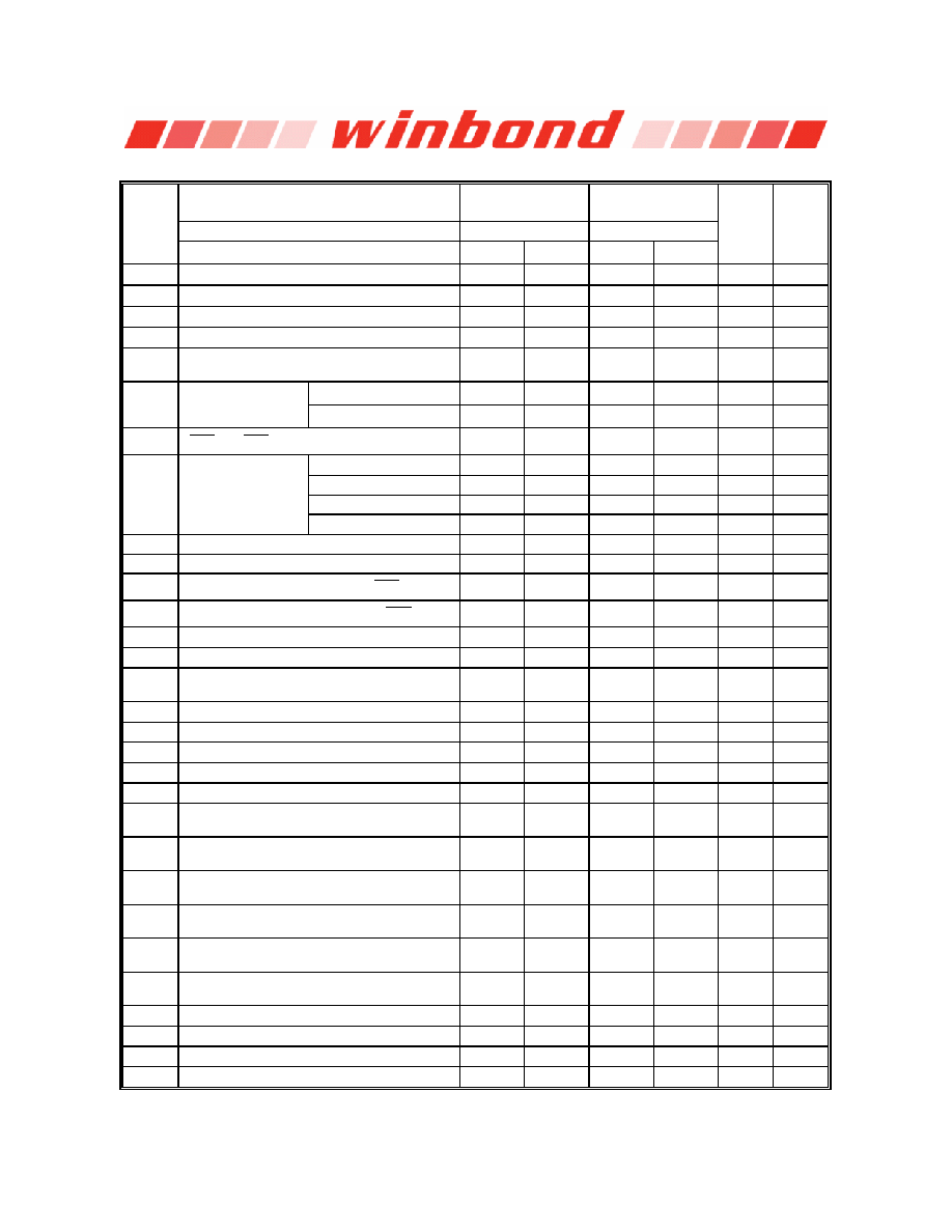
9.11.2 AC Characteristics and Operating Condition for -25/25I/-3 speed grades
SYM.
SPEED GRADE
DDR2-800
(-25/25I)
DDR2-667
(-3)
UNITS
25 NOTES
Bin(CL-tRCD-tRP)
5-5-5/6-6-6
5-5-5
PARAMETER
MIN.
MAX.
MIN.
MAX.
tRCD
Active to Read/Write Command Delay Time
12.5
15
nS
23
tRP
Precharge to Active Command Period
12.5
15
nS
23
tRC
Active to Ref/Active Command Period
52.5
55
nS
23
tRAS
Active to Precharge Command Period
40
70000
40
70000
nS
4,23
tRFC
Auto Refresh to Active/Auto Refresh command
period
75
75
nS
5
tREFI
Average periodic
refresh Interval
0°C
≤ TCASE ≤ 85°C
7.8
7.8
μS
5
85°C
< TCASE
≤ 95°C
3.9
3.9
μS
5,6
tCCD
CAS to CAS command delay
2
2
nCK
tCK(avg)
Average clock period
tCK(avg) @ CL=3
5
8
5
8
nS
30,31
tCK(avg) @ CL=4
3.75
8
3.75
8
nS
30,31
tCK(avg) @ CL=5
2.5
8
3
8
nS
30,31
tCK(avg) @ CL=6
2.5
8
nS
30,31
tCH(avg)
Average clock high pulse width
0.48
0.52
0.48
0.52
tCK(avg)
30,31
tCL(avg)
Average clock low pulse width
0.48
0.52
0.48
0.52
tCK(avg)
30,31
tAC
DQ output access time from CLK/ CLK
-400
400
-450
450
pS
35
tDQSCK
DQS output access time from CLK / CLK
-350
350
-400
400
pS
35
tDQSQ
DQS-DQ skew for DQS & associated DQ signals
200
240
pS
13
tCKE
CKE minimum high and low pulse width
3
3
nCK
7
tRRD
Active to active command period for 1KB page
size
7.5
7.5
nS
8,23
tFAW
Four Activate Window for 1KB page size
35
37.5
nS
23
tWR
Write recovery time
15
15
nS
23
tDAL
Auto-precharge write recovery + precharge time
WR + tnRP
WR + tnRP
nCK
24
tWTR
Internal Write to Read command delay
7.5
7.5
nS
9,23
tRTP
Internal Read to Precharge command delay
7.5
7.5
nS
4,23
tIS (base)
Address and control input setup time
175
200
pS
10, 26,
40,42,43
tIH (base)
Address and control input hold time
250
275
pS
11, 26,
40,42,43
tIS (ref)
Address and control input setup time
375
400
pS
10,26,
40,42,43
tIH (ref)
Address and control input hold time
375
400
pS
11,26,
40,42,43
tIPW
Address and control input pulse width for each
input
0.6
0.6
tCK(avg)
tDQSS
DQS latching rising transitions to associated
clock edges
-0.25
0.25
-0.25
0.25
tCK(avg)
28
tDSS
DQS falling edge to CLK setup time
0.2
0.2
tCK(avg)
28
tDSH
DQS falling edge hold time from CLK
0.2
0.2
tCK(avg)
28
tDQSH
DQS input high pulse width
0.35
0.35
tCK(avg)
tDQSL
DQS input low pulse width
0.35
0.35
tCK(avg)
相关PDF资料 |
PDF描述 |
|---|---|
| W972GG8JB-25I | 256M X 8 DDR DRAM, 0.4 ns, PBGA60 |
| W972GG8JB-18 | 256M X 8 DDR DRAM, 0.35 ns, PBGA60 |
| W9751G6JB-18 | 32M X 16 DDR DRAM, 0.35 ns, PBGA84 |
| W981204AH-8H | 32M X 4 SYNCHRONOUS DRAM, 6 ns, PDSO54 |
| W981216BH75L | 8M X 16 SYNCHRONOUS DRAM, 5.4 ns, PDSO54 |
相关代理商/技术参数 |
参数描述 |
|---|---|
| W9725G8JB25ITR | 制造商:Winbond Electronics Corp 功能描述:256M DDR2-800, X8, IND TEMP |
| W9725G8JB25TR | 制造商:Winbond Electronics Corp 功能描述:256M DDR2-800, X8 |
| W9725G8KB-18 | 制造商:Winbond Electronics 功能描述:IC MEMORY 制造商:Winbond Electronics Corp 功能描述:IC MEMORY |
| W9725G8KB-25 | 制造商:Winbond Electronics 功能描述:IC MEMORY 制造商:Winbond Electronics Corp 功能描述:IC MEMORY |
| W9725G8KB-25 TR | 制造商:Winbond Electronics Corp 功能描述:256M DDR2-800, X8 |
发布紧急采购,3分钟左右您将得到回复。