- 您现在的位置:买卖IC网 > PDF目录68559 > W9725G8JB-25I (WINBOND ELECTRONICS CORP) DDR DRAM, PBGA84 PDF资料下载
参数资料
| 型号: | W9725G8JB-25I |
| 厂商: | WINBOND ELECTRONICS CORP |
| 元件分类: | DRAM |
| 英文描述: | DDR DRAM, PBGA84 |
| 封装: | 8 X 12.50 MM, ROHS COMPLIANT, WBGA-84 |
| 文件页数: | 42/86页 |
| 文件大小: | 1462K |
| 代理商: | W9725G8JB-25I |
第1页第2页第3页第4页第5页第6页第7页第8页第9页第10页第11页第12页第13页第14页第15页第16页第17页第18页第19页第20页第21页第22页第23页第24页第25页第26页第27页第28页第29页第30页第31页第32页第33页第34页第35页第36页第37页第38页第39页第40页第41页当前第42页第43页第44页第45页第46页第47页第48页第49页第50页第51页第52页第53页第54页第55页第56页第57页第58页第59页第60页第61页第62页第63页第64页第65页第66页第67页第68页第69页第70页第71页第72页第73页第74页第75页第76页第77页第78页第79页第80页第81页第82页第83页第84页第85页第86页
W9725G8JB
Publication Release Date: Oct. 12, 2010
- 47 -
Revision A01
Notes:
1.
All voltages are referenced to VSS.
2.
Tests for AC timing, IDD, and electrical AC and DC characteristics may be conducted at nominal reference/supply voltage
levels, but the related specifications and device operation are guaranteed for the full voltage range specified. ODT is
disabled for all measurements that are not ODT-specific.
3.
AC timing reference load:
DQ
DQS
Output
Timing
reference
point
VTT = VDDQ/2
25
Ω
VDDQ
DUT
Figure 16
– AC timing reference load
4.
This is a minimum requirement. Minimum read to precharge timing is AL + BL / 2 provided that the tRTP and tRAS(min)
have been satisfied.
5.
If refresh timing is violated, data corruption may occur and the data must be re-written with valid data before a valid READ
can be executed.
6.
This is an optional feature. For detailed information, please refer to “operating temperature condition” section 9.2 in this data
sheet.
7.
tCKE min of 3 clocks means CKE must be registered on three consecutive positive clock edges. CKE must remain at the
valid input level the entire time it takes to achieve the 3 clocks of registration. Thus, after any CKE transition, CKE may not
transition from its valid level during the time period of tIS + 2 x tCK + tIH.
8.
A minimum of two clocks (2 *nCK) is required irrespective of operating frequency.
9.
tWTR is at least two clocks (2 * nCK) independent of operation frequency.
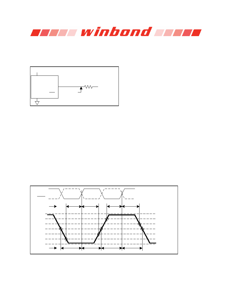
10. There are two sets of values listed for Command/Address input setup time: tIS(base) and tIS(ref). The tIS(ref) value (for
reference only) is equivalent to the baseline value of tIS(base) at VREF when the slew rate is 1.0 V/nS. The baseline value
tIS(base) is the JEDEC defined value, referenced from the input signal crossing at the VIH(ac) level for a rising signal and
VIL(ac) for a falling signal applied to the device under test. See Figure 17. If the Command/Address slew rate is not equal to
1.0 V/nS, then the baseline values must be derated by adding the values from table of tIS/tIH derating values for DDR2-667,
DDR2-800 and DDR2-1066 (page 55).
CLK
tIS(base)
tIH(base)
tIS(base)
tIH(base)
VDDQ
VIH(ac) min
VIH(dc) min
VREF(dc)
VIL(dc) max
VIL(ac) max
VSS
tIS(ref)
tIH(ref)
tIS(ref)
tIH(ref)
Logic levels
VREF levels
Figure 17
– Differential input waveform timing – tIS and tIH
相关PDF资料 |
PDF描述 |
|---|---|
| W972GG8JB-25I | 256M X 8 DDR DRAM, 0.4 ns, PBGA60 |
| W972GG8JB-18 | 256M X 8 DDR DRAM, 0.35 ns, PBGA60 |
| W9751G6JB-18 | 32M X 16 DDR DRAM, 0.35 ns, PBGA84 |
| W981204AH-8H | 32M X 4 SYNCHRONOUS DRAM, 6 ns, PDSO54 |
| W981216BH75L | 8M X 16 SYNCHRONOUS DRAM, 5.4 ns, PDSO54 |
相关代理商/技术参数 |
参数描述 |
|---|---|
| W9725G8JB25ITR | 制造商:Winbond Electronics Corp 功能描述:256M DDR2-800, X8, IND TEMP |
| W9725G8JB25TR | 制造商:Winbond Electronics Corp 功能描述:256M DDR2-800, X8 |
| W9725G8KB-18 | 制造商:Winbond Electronics 功能描述:IC MEMORY 制造商:Winbond Electronics Corp 功能描述:IC MEMORY |
| W9725G8KB-25 | 制造商:Winbond Electronics 功能描述:IC MEMORY 制造商:Winbond Electronics Corp 功能描述:IC MEMORY |
| W9725G8KB-25 TR | 制造商:Winbond Electronics Corp 功能描述:256M DDR2-800, X8 |
发布紧急采购,3分钟左右您将得到回复。