- 您现在的位置:买卖IC网 > PDF目录4101 > MT42L64M32D1KL-25 IT:A (Micron Technology Inc)IC DDR2 SDRAM 2GBIT 168FBGA PDF资料下载
参数资料
| 型号: | MT42L64M32D1KL-25 IT:A |
| 厂商: | Micron Technology Inc |
| 文件页数: | 113/164页 |
| 文件大小: | 0K |
| 描述: | IC DDR2 SDRAM 2GBIT 168FBGA |
| 标准包装: | 1,000 |
| 格式 - 存储器: | RAM |
| 存储器类型: | 移动 LPDDR2 SDRAM |
| 存储容量: | 2G(64M x 32) |
| 速度: | 400MHz |
| 接口: | 并联 |
| 电源电压: | 1.14 V ~ 1.3 V |
| 工作温度: | -25°C ~ 85°C |
| 封装/外壳: | 168-WFBGA |
| 供应商设备封装: | 168-FBGA(12x12) |
| 包装: | 散装 |
第1页第2页第3页第4页第5页第6页第7页第8页第9页第10页第11页第12页第13页第14页第15页第16页第17页第18页第19页第20页第21页第22页第23页第24页第25页第26页第27页第28页第29页第30页第31页第32页第33页第34页第35页第36页第37页第38页第39页第40页第41页第42页第43页第44页第45页第46页第47页第48页第49页第50页第51页第52页第53页第54页第55页第56页第57页第58页第59页第60页第61页第62页第63页第64页第65页第66页第67页第68页第69页第70页第71页第72页第73页第74页第75页第76页第77页第78页第79页第80页第81页第82页第83页第84页第85页第86页第87页第88页第89页第90页第91页第92页第93页第94页第95页第96页第97页第98页第99页第100页第101页第102页第103页第104页第105页第106页第107页第108页第109页第110页第111页第112页当前第113页第114页第115页第116页第117页第118页第119页第120页第121页第122页第123页第124页第125页第126页第127页第128页第129页第130页第131页第132页第133页第134页第135页第136页第137页第138页第139页第140页第141页第142页第143页第144页第145页第146页第147页第148页第149页第150页第151页第152页第153页第154页第155页第156页第157页第158页第159页第160页第161页第162页第163页第164页
�� �
�
�2Gb:� x16,� x32� Mobile� LPDDR2� SDRAM� S4�
�Electrical� Specifications�
�Electrical� Specifications�
�Absolute� Maximum� Ratings�
�Stresses� greater� than� those� listed� below� may� cause� permanent� damage� to� the� device.�
�This� is� a� stress� rating� only,� and� functional� operation� of� the� device� at� these� or� any� other�
�conditions� outside� those� indicated� in� the� operational� sections� of� this� document� is� not�
�implied.� Exposure� to� absolute� maximum� rating� conditions� for� extended� periods� may�
�adversely� affect� reliability.�
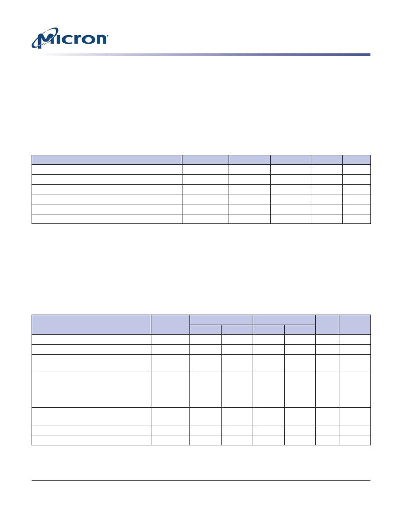
�Table� 54:� Absolute� Maximum� DC� Ratings�
�Parameter�
�V� DD1� supply� voltage� relative� to� V� SS�
�V� DD2� supply� voltage� relative� to� V� SS�
�V� DDCA� supply� voltage� relative� to� V� SSCA�
�V� DDQ� supply� voltage� relative� to� V� SSQ�
�Voltage� on� any� ball� relative� to� V� SS�
�Storage� temperature�
�Symbol�
�V� DD1�
�V� DD2� (1.2V)�
�V� DDCA�
�V� DDQ�
�V� IN� ,� V� OUT�
�T� STG�
�Min�
�–0.4�
�–0.4�
�–0.4�
�–0.4�
�–0.4�
�–55�
�Max�
�+2.3�
�+1.6�
�+1.6�
�+1.6�
�+1.6�
�+125�
�Unit�
�V�
�V�
�V�
�V�
�V�
�?C�
�Notes�
�1�
�1�
�1,� 2�
�1,� 3�
�4�
�Notes:�
�1.�
�2.�
�3.�
�4.�
�See� 1.� Voltage� Ramp� under� Power-Up� (page� 40).�
�V� REFCA� 0.6� ≤� V� DDCA� ;� however,� V� REFCA� may� be� ≥� V� DDCA� provided� that� V� REFCA� ≤� 300mV.�
�V� REFDQ� 0.6� ≤� V� DDQ� ;� however,� V� REFDQ� may� be� ≥� V� DDQ� provided� that� V� REFDQ� ≤� 300mV.�
�Storage� temperature� is� the� case� surface� temperature� on� the� center/top� side� of� the� de-�
�vice.� For� measurement� conditions,� refer� to� the� JESD51-2� standard.�
�Input/Output� Capacitance�
�Table� 55:� Input/Output� Capacitance�
�Note� 1� applies� to� all� parameters� and� conditions�
�LPDDR2� 1066-466�
�LPDDR2� 400-200�
�Parameter�
�Input� capacitance,� CK� and� CK#�
�Input� capacitance� delta,� CK� and� CK#�
�Input� capacitance,� all� other� input-�
�Symbol�
�C� CK�
�C� DCK�
�C� I�
�MIN�
�1.0�
�0�
�1.0�
�MAX�
�2.0�
�0.20�
�2.0�
�MIN�
�1.0�
�0�
�1.0�
�MAX�
�2.0�
�0.25�
�2.0�
�Unit�
�pF�
�pF�
�pF�
�Notes�
�2,� 3�
�2,� 3,� 4�
�2,� 3,� 5�
�only� pins�
�Input� capacitance� delta,� all� other� input-�
�C� DI�
�–0.40�
�+0.40�
�–0.50�
�+0.50�
�pF�
�2,� 3,� 6�
�only� pins�
�Input/output� capacitance,� DQ,� DM,� DQS,�
�C� IO�
�1.25�
�2.5�
�1.25�
�2.5�
�pF�
�2,� 3,� 7,� 8�
�DQS#�
�Input/output� capacitance� delta,� DQS,�
�C� DDQS�
�0�
�0.25�
�0�
�0.30�
�pF�
�2,� 3,� 8,� 9�
�DQS#�
�Input/output� capacitance� delta,� DQ,� DM�
�Input/output� capacitance� ZQ�
�C� DIO�
�C� ZQ�
�–0.5�
�0�
�+0.5�
�2.5�
�–0.6�
�0�
�+0.6�
�2.5�
�pF�
�pF�
�2,� 3,� 8,� 10�
�2,� 3,� 11�
�Notes:�
�1.� T� C� –25?C� to� +105?C;� V� DDQ� =� 1.14–1.3V;� V� DDCA� =� 1.14–1.3V;� V� DD1� =� 1.7–1.95V;� V� DD2� =� 1.14–�
�1.3V.�
�PDF:� 09005aef83f3f2eb�
�2gb_mobile_lpddr2_s4_g69a.pdf� –� Rev.� N� 3/12� EN�
�113�
�Micron� Technology,� Inc.� reserves� the� right� to� change� products� or� specifications� without� notice.�
�2010� Micron� Technology,� Inc.� All� rights� reserved.�
�相关PDF资料 |
PDF描述 |
|---|---|
| IDT71V67803S133BQG8 | IC SRAM 9MBIT 133MHZ 165FBGA |
| IDT71V65803S150PFG | IC SRAM 9MBIT 150MHZ 100TQFP |
| IDT71V67903S85BQI8 | IC SRAM 9MBIT 85NS 165FBGA |
| IDT71V67903S80BQI8 | IC SRAM 9MBIT 80NS 165FBGA |
| IDT71V67903S75BQI8 | IC SRAM 9MBIT 75NS 165FBGA |
相关代理商/技术参数 |
参数描述 |
|---|
发布紧急采购,3分钟左右您将得到回复。