- 您现在的位置:买卖IC网 > PDF目录4101 > MT42L64M32D1KL-25 IT:A (Micron Technology Inc)IC DDR2 SDRAM 2GBIT 168FBGA PDF资料下载
参数资料
| 型号: | MT42L64M32D1KL-25 IT:A |
| 厂商: | Micron Technology Inc |
| 文件页数: | 39/164页 |
| 文件大小: | 0K |
| 描述: | IC DDR2 SDRAM 2GBIT 168FBGA |
| 标准包装: | 1,000 |
| 格式 - 存储器: | RAM |
| 存储器类型: | 移动 LPDDR2 SDRAM |
| 存储容量: | 2G(64M x 32) |
| 速度: | 400MHz |
| 接口: | 并联 |
| 电源电压: | 1.14 V ~ 1.3 V |
| 工作温度: | -25°C ~ 85°C |
| 封装/外壳: | 168-WFBGA |
| 供应商设备封装: | 168-FBGA(12x12) |
| 包装: | 散装 |
第1页第2页第3页第4页第5页第6页第7页第8页第9页第10页第11页第12页第13页第14页第15页第16页第17页第18页第19页第20页第21页第22页第23页第24页第25页第26页第27页第28页第29页第30页第31页第32页第33页第34页第35页第36页第37页第38页当前第39页第40页第41页第42页第43页第44页第45页第46页第47页第48页第49页第50页第51页第52页第53页第54页第55页第56页第57页第58页第59页第60页第61页第62页第63页第64页第65页第66页第67页第68页第69页第70页第71页第72页第73页第74页第75页第76页第77页第78页第79页第80页第81页第82页第83页第84页第85页第86页第87页第88页第89页第90页第91页第92页第93页第94页第95页第96页第97页第98页第99页第100页第101页第102页第103页第104页第105页第106页第107页第108页第109页第110页第111页第112页第113页第114页第115页第116页第117页第118页第119页第120页第121页第122页第123页第124页第125页第126页第127页第128页第129页第130页第131页第132页第133页第134页第135页第136页第137页第138页第139页第140页第141页第142页第143页第144页第145页第146页第147页第148页第149页第150页第151页第152页第153页第154页第155页第156页第157页第158页第159页第160页第161页第162页第163页第164页
�� �
�
�2Gb:� x16,� x32� Mobile� LPDDR2� SDRAM� S4�
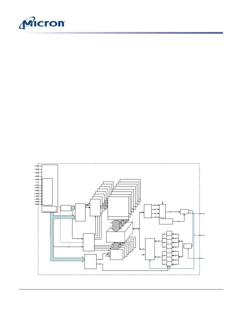
�Functional� Description�
�Functional� Description�
�Mobile� LPDDR2� is� a� high-speed� SDRAM� internally� configured� as� a� 4-� or� 8-bank� memory�
�device.� LPDDR2� devices� use� a� double� data� rate� architecture� on� the� command/address�
�(CA)� bus� to� reduce� the� number� of� input� pins� in� the� system.� The� 10-bit� CA� bus� is� used� to�
�transmit� command,� address,� and� bank� information.� Each� command� uses� one� clock� cy-�
�cle,� during� which� command� information� is� transferred� on� both� the� rising� and� falling�
�edges� of� the� clock.�
�LPDDR2-S4� devices� use� a� double� data� rate� architecture� on� the� DQ� pins� to� achieve� high-�
�speed� operation.� The� double� data� rate� architecture� is� essentially� a� 4� n� prefetch� architec-�
�ture� with� an� interface� designed� to� transfer� two� data� bits� per� DQ� every� clock� cycle� at� the�
�I/O� pins.� A� single� read� or� write� access� for� the� LPDDR2-S4� effectively� consists� of� a� single�
�4� n� -bit-wide,� one-clock-cycle� data� transfer� at� the� internal� SDRAM� core� and� four� corre-�
�sponding� n� -bit-wide,� one-half-clock-cycle� data� transfers� at� the� I/O� pins.�
�Read� and� write� accesses� are� burst� oriented;� accesses� start� at� a� selected� location� and�
�continue� for� a� programmed� number� of� locations� in� a� programmed� sequence.�
�Accesses� begin� with� the� registration� of� an� ACTIVATE� command� followed� by� a� READ� or�
�WRITE� command.� The� address� and� BA� bits� registered� coincident� with� the� ACTIVATE�
�command� are� used� to� select� the� row� and� bank� to� be� accessed.� The� address� bits� regis-�
�tered� coincident� with� the� READ� or� WRITE� command� are� used� to� select� the� bank� and� the�
�starting� column� location� for� the� burst� access.�
�Figure� 25:� Functional� Block� Diagram�
�CKE�
�CK�
�CK#�
�CS#�
�Control�
�logic�
�CA0�
�CA1�
�CA2�
�CA3�
�CA4�
�Bank� 7�
�Bank� 6�
�Bank� 5�
�Bank� 4�
�Bank� 7�
�Bank� 6�
�Bank� 5�
�Bank� 4�
�Bank� 3�
�CA5�
�CA6�
�CA7�
�CA8�
�CA9�
�Mode�
�registers�
�Refresh� x�
�counter�
�Row-�
�address�
�MUX�
�x�
�Bank� 3�
�Bank� 2�
�Bank� 1�
�Bank� 0�
�row-�
�address�
�latch�
�and�
�decoder�
�Bank� 2�
�Bank� 1�
�Bank� 0�
�Memory� array�
�4n�
�Read�
�latch�
�n�
�n�
�n�
�n�
�COL0�
�MUX�
�n�
�DATA�
�DRVRS�
�DQ0–DQn-1�
�Sense� amplifier�
�DQS�
�generator�
�DQS,� DQS#�
�4n�
�Input�
�registers�
�4�
�4�
�3�
�3�
�Bank�
�control�
�logic�
�I/O� gating�
�DM� mask� logic�
�4n�
�WRITE�
�FIFO�
�and�
�drivers�
�8�
�Mask�
�4�
�4�
�4�
�n�
�4�
�4�
�4�
�n�
�4�
�RCVRS�
�DQS,� DQS#�
�counter/�
�Column-� y� -� 1�
�address�
�1�
�Column�
�decoder�
�CK,� CK#�
�CK� out�
�CK� in�
�4n�
�Data�
�n�
�n�
�n�
�n�
�n�
�n�
�n�
�DM�
�latch�
�COL0�
�PDF:� 09005aef83f3f2eb�
�2gb_mobile_lpddr2_s4_g69a.pdf� –� Rev.� N� 3/12� EN�
�39�
�Micron� Technology,� Inc.� reserves� the� right� to� change� products� or� specifications� without� notice.�
�2010� Micron� Technology,� Inc.� All� rights� reserved.�
�相关PDF资料 |
PDF描述 |
|---|---|
| IDT71V67803S133BQG8 | IC SRAM 9MBIT 133MHZ 165FBGA |
| IDT71V65803S150PFG | IC SRAM 9MBIT 150MHZ 100TQFP |
| IDT71V67903S85BQI8 | IC SRAM 9MBIT 85NS 165FBGA |
| IDT71V67903S80BQI8 | IC SRAM 9MBIT 80NS 165FBGA |
| IDT71V67903S75BQI8 | IC SRAM 9MBIT 75NS 165FBGA |
相关代理商/技术参数 |
参数描述 |
|---|
发布紧急采购,3分钟左右您将得到回复。