- 您现在的位置:买卖IC网 > PDF目录4101 > MT42L64M32D1KL-25 IT:A (Micron Technology Inc)IC DDR2 SDRAM 2GBIT 168FBGA PDF资料下载
参数资料
| 型号: | MT42L64M32D1KL-25 IT:A |
| 厂商: | Micron Technology Inc |
| 文件页数: | 83/164页 |
| 文件大小: | 0K |
| 描述: | IC DDR2 SDRAM 2GBIT 168FBGA |
| 标准包装: | 1,000 |
| 格式 - 存储器: | RAM |
| 存储器类型: | 移动 LPDDR2 SDRAM |
| 存储容量: | 2G(64M x 32) |
| 速度: | 400MHz |
| 接口: | 并联 |
| 电源电压: | 1.14 V ~ 1.3 V |
| 工作温度: | -25°C ~ 85°C |
| 封装/外壳: | 168-WFBGA |
| 供应商设备封装: | 168-FBGA(12x12) |
| 包装: | 散装 |
第1页第2页第3页第4页第5页第6页第7页第8页第9页第10页第11页第12页第13页第14页第15页第16页第17页第18页第19页第20页第21页第22页第23页第24页第25页第26页第27页第28页第29页第30页第31页第32页第33页第34页第35页第36页第37页第38页第39页第40页第41页第42页第43页第44页第45页第46页第47页第48页第49页第50页第51页第52页第53页第54页第55页第56页第57页第58页第59页第60页第61页第62页第63页第64页第65页第66页第67页第68页第69页第70页第71页第72页第73页第74页第75页第76页第77页第78页第79页第80页第81页第82页当前第83页第84页第85页第86页第87页第88页第89页第90页第91页第92页第93页第94页第95页第96页第97页第98页第99页第100页第101页第102页第103页第104页第105页第106页第107页第108页第109页第110页第111页第112页第113页第114页第115页第116页第117页第118页第119页第120页第121页第122页第123页第124页第125页第126页第127页第128页第129页第130页第131页第132页第133页第134页第135页第136页第137页第138页第139页第140页第141页第142页第143页第144页第145页第146页第147页第148页第149页第150页第151页第152页第153页第154页第155页第156页第157页第158页第159页第160页第161页第162页第163页第164页
�� �
�
�2Gb:� x16,� x32� Mobile� LPDDR2� SDRAM� S4�
�SELF� REFRESH� Operation�
�self� refresh� entry� is� registered;� however,� the� clock� must� be� restarted� and� stable� before�
�the� device� can� exit� SELF� REFRESH� operation.�
�Exiting� self� refresh� requires� a� series� of� commands.� First,� the� clock� must� be� stable� prior�
�to� CKE� returning� HIGH.� After� the� self� refresh� exit� is� registered,� a� minimum� delay,� at� least�
�equal� to� the� self� refresh� exit� interval� (� t� XSR),� must� be� satisfied� before� a� valid� command�
�can� be� issued� to� the� device.� This� provides� completion� time� for� any� internal� refresh� in�
�progress.� For� proper� operation,� CKE� must� remain� HIGH� throughout� t� XSR,� except� during�
�self� refresh� re-entry.� NOP� commands� must� be� registered� on� each� rising� clock� edge� dur-�
�ing� t� XSR.�
�Using� self� refresh� mode� introduces� the� possibility� that� an� internally� timed� refresh� event�
�could� be� missed� when� CKE� is� driven� HIGH� for� exit� from� self� refresh� mode.� Upon� exiting�
�self� refresh,� at� least� one� REFRESH� command� (one� all-bank� command� or� eight� per-bank�
�commands)� must� be� issued� before� issuing� a� subsequent� SELF� REFRESH� command.�
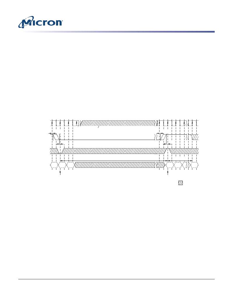
�Figure� 60:� SELF� REFRESH� Operation�
�CK/CK#�
�CKE�
�CS#�
�tIHCKE�
�tISCKE�
�Input� clock� frequency� can� be� changed�
�or� clock� can� be� stopped� during� self� refresh.�
�tCKESR� (MIN)�
�tIHCKE�
�tISCKE�
�tXSR� (MIN)�
�Valid� Enter� NOP�
�CMD�
�SR�
�Exit�
�SR�
�NOP� NOP� Valid�
�Enter� self� refresh� mode�
�Exit� self� refresh� mode�
�Don’t� Care�
�Notes:�
�1.� Input� clock� frequency� can� be� changed� or� stopped� during� self� refresh,� provided� that�
�upon� exiting� self-refresh,� a� minimum� of� two� cycles� of� stable� clocks� are� provided,� and� the�
�clock� frequency� is� between� the� minimum� and� maximum� frequencies� for� the� particular�
�speed� grade.�
�2.� The� device� must� be� in� the� all� banks� idle� state� prior� to� entering� self� refresh� mode.�
�3.� t� XSR� begins� at� the� rising� edge� of� the� clock� after� CKE� is� driven� HIGH.�
�4.� A� valid� command� can� be� issued� only� after� t� XSR� is� satisfied.� NOPs� must� be� issued� during�
�t� XSR.�
�Partial-Array� Self� Refresh� –� Bank� Masking�
�Devices� in� densities� of� 64Mb–512Mb� are� comprised� of� four� banks;� densities� of� 1Gb� and�
�higher� are� comprised� of� eight� banks.� Each� bank� can� be� configured� independently�
�whether� or� not� a� SELF� REFRESH� operation� will� occur� in� that� bank.� One� 8-bit� mode� reg-�
�ister� (accessible� via� the� MRW� command)� is� assigned� to� program� the� bank-masking� sta-�
�tus� of� each� bank� up� to� eight� banks.� For� bank� masking� bit� assignments,� see� the� MR16�
�PASR� Bank� Mask� (MA[7:0]� =� 010h)� and� MR16� Op-Code� Bit� Definitions� tables.�
�PDF:� 09005aef83f3f2eb�
�2gb_mobile_lpddr2_s4_g69a.pdf� –� Rev.� N� 3/12� EN�
�83�
�Micron� Technology,� Inc.� reserves� the� right� to� change� products� or� specifications� without� notice.�
�2010� Micron� Technology,� Inc.� All� rights� reserved.�
�相关PDF资料 |
PDF描述 |
|---|---|
| IDT71V67803S133BQG8 | IC SRAM 9MBIT 133MHZ 165FBGA |
| IDT71V65803S150PFG | IC SRAM 9MBIT 150MHZ 100TQFP |
| IDT71V67903S85BQI8 | IC SRAM 9MBIT 85NS 165FBGA |
| IDT71V67903S80BQI8 | IC SRAM 9MBIT 80NS 165FBGA |
| IDT71V67903S75BQI8 | IC SRAM 9MBIT 75NS 165FBGA |
相关代理商/技术参数 |
参数描述 |
|---|
发布紧急采购,3分钟左右您将得到回复。