- 您现在的位置:买卖IC网 > PDF目录385639 > MT48V4M32LFFC (Micron Technology, Inc.) SYNCHRONOUS DRAM PDF资料下载
参数资料
| 型号: | MT48V4M32LFFC |
| 厂商: | Micron Technology, Inc. |
| 英文描述: | SYNCHRONOUS DRAM |
| 中文描述: | 同步DRAM |
| 文件页数: | 11/61页 |
| 文件大小: | 1400K |
| 代理商: | MT48V4M32LFFC |
第1页第2页第3页第4页第5页第6页第7页第8页第9页第10页当前第11页第12页第13页第14页第15页第16页第17页第18页第19页第20页第21页第22页第23页第24页第25页第26页第27页第28页第29页第30页第31页第32页第33页第34页第35页第36页第37页第38页第39页第40页第41页第42页第43页第44页第45页第46页第47页第48页第49页第50页第51页第52页第53页第54页第55页第56页第57页第58页第59页第60页第61页
11
128Mb: x16, x32 Mobile SDRAM
MobileY95W_3V_F.p65 – Rev. F; Pub. 9/02
Micron Technology, Inc., reserves the right to change products or specifications without notice.
2002, Micron Technology, Inc.
128Mb: x16, x32
MOBILE SDRAM
ADVANCE
ALLOWABLE OPERATING
FREQUENCY (MHz)
CAS
LATENCY = 1
LATENCY = 2
≤
50
≤
40
CAS
CAS
SPEED
- 8
- 10
LATENCY = 3
≤
125
≤
100
≤
100
≤
83
Operating Mode
The normal operating mode is selected by setting M7
and M8 to zero; the other combinations of values for M7
and M8 are reserved for future use and/or test modes.
The programmed burst length applies to both READ and
WRITE bursts.
Test modes and reserved states should not be used
because unknown operation or incompatibility with fu-
ture versions may result.
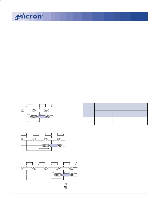
CAS Latency
The CAS latency is the delay, in clock cycles, between
the registration of a READ command and the availability
of the first piece of output data. The latency can be set to
one, two, or three clocks.
If a READ command is registered at clock edge
n
, and
the latency is
m
clocks, the data will be available by clock
edge
n + m
. The DQs will start driving as a result of the
clock edge one cycle earlier (
n + m
- 1), and provided that
the relevant access times are met, the data will be valid by
clock edge
n + m
. For example, assuming that the clock
cycle time is such that all relevant access times are met,
if a READ command is registered at T0 and the latency is
programmed to two clocks, the DQs will start driving
after T1 and the data will be valid by T2, as shown in
Figure 2. Table 2 indicates the operating frequencies at
which each CAS latency setting can be used.
Reserved states should not be used as unknown op-
eration or incompatibility with future versions
may result.
Figure 2
CAS Latency
Table 2
CAS Latency
CLK
DQ
T2
T1
T3
T0
CAS Latency = 3
LZ
t
D
OUT
tOH
COMMAND
NOP
READ
tAC
NOP
T4
NOP
DON’T CARE
UNDEFINED
CLK
DQ
T2
T1
T0
CAS Latency = 1
LZ
t
D
OUT
tOH
COMMAND
NOP
READ
tAC
CLK
DQ
T2
T1
T3
T0
CAS Latency = 2
LZ
t
D
OUT
tOH
COMMAND
NOP
READ
tAC
NOP
相关PDF资料 |
PDF描述 |
|---|---|
| MT49H16M16 | THERMISTOR PTC 100OHM 110DEG RAD |
| MT49H16M16FM | REDUCED LATENCY DRAM RLDRAM |
| MT49H8M32 | THERMISTOR PTC 100OHM 120DEG RAD |
| MT49H8M32FM | REDUCED LATENCY DRAM RLDRAM |
| MT4C1M16E5DJ-6 | EDO DRAM |
相关代理商/技术参数 |
参数描述 |
|---|
发布紧急采购,3分钟左右您将得到回复。