- 您现在的位置:买卖IC网 > PDF目录385639 > MT48V4M32LFFC (Micron Technology, Inc.) SYNCHRONOUS DRAM PDF资料下载
参数资料
| 型号: | MT48V4M32LFFC |
| 厂商: | Micron Technology, Inc. |
| 英文描述: | SYNCHRONOUS DRAM |
| 中文描述: | 同步DRAM |
| 文件页数: | 19/61页 |
| 文件大小: | 1400K |
| 代理商: | MT48V4M32LFFC |
第1页第2页第3页第4页第5页第6页第7页第8页第9页第10页第11页第12页第13页第14页第15页第16页第17页第18页当前第19页第20页第21页第22页第23页第24页第25页第26页第27页第28页第29页第30页第31页第32页第33页第34页第35页第36页第37页第38页第39页第40页第41页第42页第43页第44页第45页第46页第47页第48页第49页第50页第51页第52页第53页第54页第55页第56页第57页第58页第59页第60页第61页
19
128Mb: x16, x32 Mobile SDRAM
MobileY95W_3V_F.p65 – Rev. F; Pub. 9/02
Micron Technology, Inc., reserves the right to change products or specifications without notice.
2002, Micron Technology, Inc.
128Mb: x16, x32
MOBILE SDRAM
ADVANCE
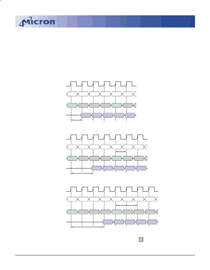
This is shown in Figure 7 for CAS latencies of two and
three; data element
n
+ 3 is either the last of a burst of four
or the last desired of a longer burst. The 128Mb SDRAM
uses a pipelined architecture and therefore does not
require the 2
n
rule associated with a prefetch architec-
Figure 7
Consecutive READ Bursts
ture. A READ command can be initiated on any clock
cycle following a previous READ command. Full-speed
random read accesses can be performed to the same
bank, as shown in Figure 8, or each subsequent READ
may be performed to a different bank.
CLK
DQ
D
OUT
n
T2
T1
T4
T3
T5
T0
COMMAND
ADDRESS
READ
NOP
NOP
NOP
BANK,
COL
n
NOP
BANK,
COL
b
D
OUT
n
+ 1
D
OUT
n
+ 2
D
OUT
n
+ 3
D
OUT
b
READ
X
= 0 cycles
NOTE:
Each READ command may be to either bank. DQM is LOW.
CAS Latency = 1
CLK
DQ
D
OUT
n
T2
T1
T4
T3
T6
T5
T0
COMMAND
ADDRESS
READ
NOP
NOP
NOP
NOP
BANK,
COL
n
NOP
BANK,
COL
b
D
OUT
n
+ 1
D
OUT
n
+ 2
D
OUT
n
+ 3
D
OUT
b
READ
X
= 1 cycle
CAS Latency = 2
CLK
DQ
D
OUT
n
T2
T1
T4
T3
T6
T5
T0
COMMAND
ADDRESS
READ
NOP
NOP
NOP
NOP
BANK,
COL n
NOP
BANK,
COL
b
D
OUT
n
+ 1
D
OUT
n
+ 2
D
OUT
n
+ 3
D
OUT
b
READ
NOP
T7
X
= 2 cycles
CAS Latency = 3
DON’T CARE
相关PDF资料 |
PDF描述 |
|---|---|
| MT49H16M16 | THERMISTOR PTC 100OHM 110DEG RAD |
| MT49H16M16FM | REDUCED LATENCY DRAM RLDRAM |
| MT49H8M32 | THERMISTOR PTC 100OHM 120DEG RAD |
| MT49H8M32FM | REDUCED LATENCY DRAM RLDRAM |
| MT4C1M16E5DJ-6 | EDO DRAM |
相关代理商/技术参数 |
参数描述 |
|---|
发布紧急采购,3分钟左右您将得到回复。