- 您现在的位置:买卖IC网 > PDF目录202173 > V59C1G01808QALF19E (PROMOS TECHNOLOGIES INC) 128M X 8 DDR DRAM, BGA68 PDF资料下载
参数资料
| 型号: | V59C1G01808QALF19E |
| 厂商: | PROMOS TECHNOLOGIES INC |
| 元件分类: | DRAM |
| 英文描述: | 128M X 8 DDR DRAM, BGA68 |
| 封装: | ROHS COMPLIANT, FBGA-68 |
| 文件页数: | 26/79页 |
| 文件大小: | 1028K |
| 代理商: | V59C1G01808QALF19E |
第1页第2页第3页第4页第5页第6页第7页第8页第9页第10页第11页第12页第13页第14页第15页第16页第17页第18页第19页第20页第21页第22页第23页第24页第25页当前第26页第27页第28页第29页第30页第31页第32页第33页第34页第35页第36页第37页第38页第39页第40页第41页第42页第43页第44页第45页第46页第47页第48页第49页第50页第51页第52页第53页第54页第55页第56页第57页第58页第59页第60页第61页第62页第63页第64页第65页第66页第67页第68页第69页第70页第71页第72页第73页第74页第75页第76页第77页第78页第79页
32
V59C1G01(408/808/168)QA Rev. 1.3 June 2008
ProMOS TECHNOLOGIES
V59C1G01(408/808/168)QA
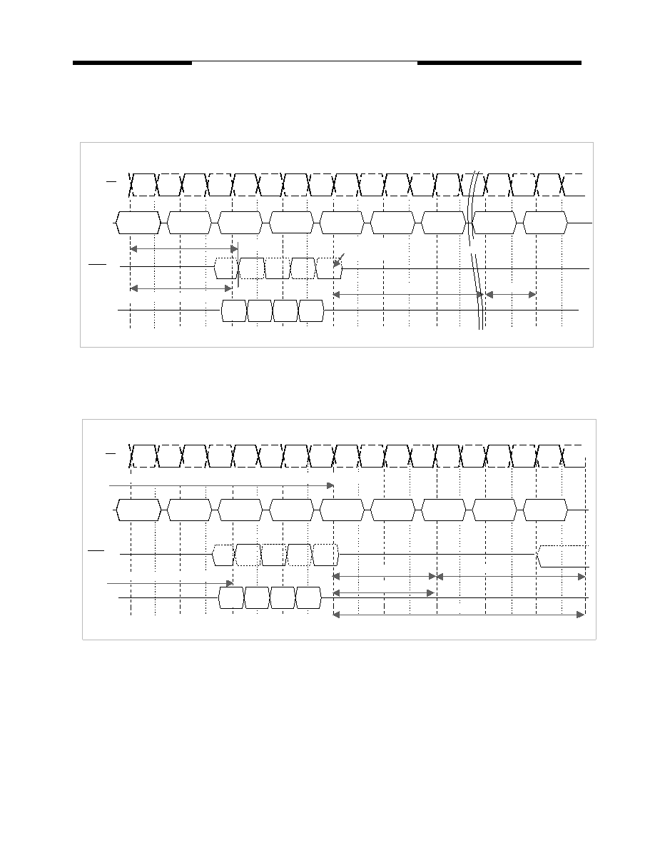
Burst Write Operation : RL = 3 (AL = 0, CL = 3), WL = 2, BL = 4
NOP
WRITE A
Post CAS
T0
T2
T1
T3
T4
T5
T6
Tm
Tn
WL = RL-1 = 2
BW322
CMD
DQ
NOP
DIN A0 DIN A1 DIN A2 DIN A3
tWR
Completion of
the Burst Write
<= tDQSS
Precharge
Bank A
Activate
tRP
DQS,
DQS
CK, CK
Burst Write followed by Burst Read : RL = 5 (AL = 2, CL = 3), WL = 4, tWTR = 2, BL = 4
NOP
READ A
Post CAS
BWBR
CMD
DQ
NOP
DIN A0 DIN A1 DIN A2 DIN A3
AL=2
CL=3
NOP
tWTR
T0
T2
T1
T3
T4
T5
T6
T7
T8
T9
Write to Read = (CL - 1)+ BL/2 +tWTR(2) = 6
DQS,
DQS
WL = RL - 1 = 4
RL=5
CK, CK
The minimum number of clocks from the burst write command to the burst read command is
(CL - 1) +BL/2 + tWTR
where tWTR is the write-to-read turn-around time tWTR expressed in clock cycles. The tWTR is not a write
recovery time (tWR) but the time required to transfer 4 bit write data from the input buffer into sense amplifiers
in the array.
相关PDF资料 |
PDF描述 |
|---|---|
| V59C1G01808QALF37E | 128M X 8 DDR DRAM, BGA68 |
| V59C1G01808QAUF37H | 128M X 8 DDR DRAM, PBGA68 |
| V59C1512804QALP19A | 64M X 8 DDR DRAM, PBGA68 |
| V59C1512804QAUF19AI | 64M X 8 DDR DRAM, PBGA68 |
| V59C1512804QAUP19AH | 64M X 8 DDR DRAM, PBGA68 |
相关代理商/技术参数 |
参数描述 |
|---|---|
| V5A010CB | 制造商:Honeywell Sensing and Control 功能描述:MICROSWITCH V5 PIN PLUNGER |
| V5A010CB | 制造商:Honeywell Sensing and Control 功能描述:MICROSWITCH V5 PIN PLUNGER |
| V5A010CB4D | 制造商:Honeywell Sensing and Control 功能描述:MICROSWITCH V5 ROLLER LEVER |
| V5A010CB4D | 制造商:Honeywell Sensing and Control 功能描述:MICROSWITCH V5 ROLLER LEVER |
| V5A010CB4E | 制造商:Honeywell Sensing and Control 功能描述:MICROSWITCH V5 ROLLER LEVER |
发布紧急采购,3分钟左右您将得到回复。