- 您现在的位置:买卖IC网 > PDF目录202173 > V59C1G01808QALF19E (PROMOS TECHNOLOGIES INC) 128M X 8 DDR DRAM, BGA68 PDF资料下载
参数资料
| 型号: | V59C1G01808QALF19E |
| 厂商: | PROMOS TECHNOLOGIES INC |
| 元件分类: | DRAM |
| 英文描述: | 128M X 8 DDR DRAM, BGA68 |
| 封装: | ROHS COMPLIANT, FBGA-68 |
| 文件页数: | 28/79页 |
| 文件大小: | 1028K |
| 代理商: | V59C1G01808QALF19E |
第1页第2页第3页第4页第5页第6页第7页第8页第9页第10页第11页第12页第13页第14页第15页第16页第17页第18页第19页第20页第21页第22页第23页第24页第25页第26页第27页当前第28页第29页第30页第31页第32页第33页第34页第35页第36页第37页第38页第39页第40页第41页第42页第43页第44页第45页第46页第47页第48页第49页第50页第51页第52页第53页第54页第55页第56页第57页第58页第59页第60页第61页第62页第63页第64页第65页第66页第67页第68页第69页第70页第71页第72页第73页第74页第75页第76页第77页第78页第79页
34
V59C1G01(408/808/168)QA Rev. 1.3 June 2008
ProMOS TECHNOLOGIES
V59C1G01(408/808/168)QA
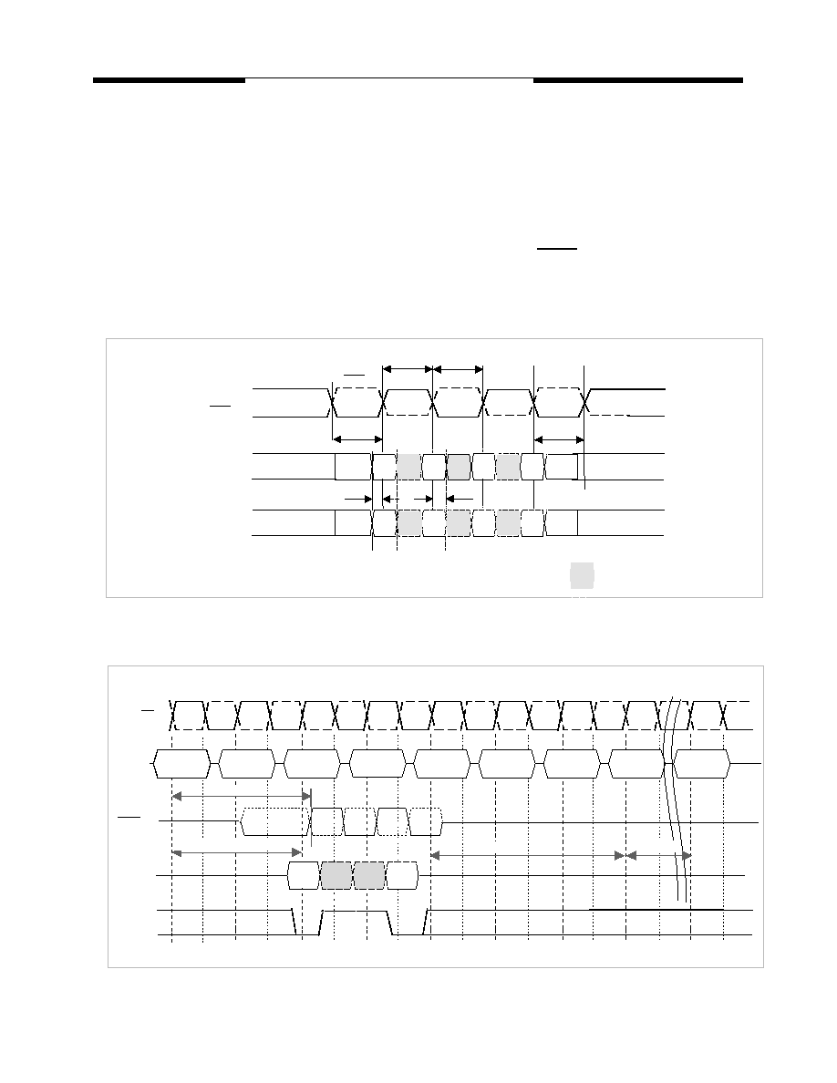
Write Data Mask
One write data mask input (DM) for x4 and x8 components and two write data mask inputs (LDM, UDM) for
x16 components are supported on DDR2 SDRAMs, consistent with the implementation on DDR SDRAMs. It
has identical timings on write operations as the data bits, and though used in a uni-directional manner, is
internally loaded identically to data bits to insure matched system timing. Data mask is not used during read
cycles. If DM is high during a write burst coincident with the write data, the write data bit is not written to the
memory. For x8 components the DM function is disabled, when RDQS / RDQS are enabled by EMRS.
.
Write Data Mask Timing
DQS,
DQS
t DQSH
tDQSL
t WPRE
WPST
t
DQ
Din
tDS
DH
DM
don’t care
Din
t
.
Burst Write Operation with Data Mask : RL = 3 (AL = 0, CL = 3), WL = 2, tWR = 3 , BL = 4
NOP
WRITE A
T0
T2
T1
T3
T4
T5
T6
T7
Tn
WL = RL-1 = 2
DM
CMD
DQ
NOP
tWR
<= tDQSS
Precharge
Bank A
Activate
tRP
DQS,
DQS
DM
DIN A0
DIN A3
CK, CK
DIN A1 DIN A2
相关PDF资料 |
PDF描述 |
|---|---|
| V59C1G01808QALF37E | 128M X 8 DDR DRAM, BGA68 |
| V59C1G01808QAUF37H | 128M X 8 DDR DRAM, PBGA68 |
| V59C1512804QALP19A | 64M X 8 DDR DRAM, PBGA68 |
| V59C1512804QAUF19AI | 64M X 8 DDR DRAM, PBGA68 |
| V59C1512804QAUP19AH | 64M X 8 DDR DRAM, PBGA68 |
相关代理商/技术参数 |
参数描述 |
|---|---|
| V5A010CB | 制造商:Honeywell Sensing and Control 功能描述:MICROSWITCH V5 PIN PLUNGER |
| V5A010CB | 制造商:Honeywell Sensing and Control 功能描述:MICROSWITCH V5 PIN PLUNGER |
| V5A010CB4D | 制造商:Honeywell Sensing and Control 功能描述:MICROSWITCH V5 ROLLER LEVER |
| V5A010CB4D | 制造商:Honeywell Sensing and Control 功能描述:MICROSWITCH V5 ROLLER LEVER |
| V5A010CB4E | 制造商:Honeywell Sensing and Control 功能描述:MICROSWITCH V5 ROLLER LEVER |
发布紧急采购,3分钟左右您将得到回复。