- 您现在的位置:买卖IC网 > PDF目录202173 > V59C1G01808QALF19E (PROMOS TECHNOLOGIES INC) 128M X 8 DDR DRAM, BGA68 PDF资料下载
参数资料
| 型号: | V59C1G01808QALF19E |
| 厂商: | PROMOS TECHNOLOGIES INC |
| 元件分类: | DRAM |
| 英文描述: | 128M X 8 DDR DRAM, BGA68 |
| 封装: | ROHS COMPLIANT, FBGA-68 |
| 文件页数: | 31/79页 |
| 文件大小: | 1028K |
| 代理商: | V59C1G01808QALF19E |
第1页第2页第3页第4页第5页第6页第7页第8页第9页第10页第11页第12页第13页第14页第15页第16页第17页第18页第19页第20页第21页第22页第23页第24页第25页第26页第27页第28页第29页第30页当前第31页第32页第33页第34页第35页第36页第37页第38页第39页第40页第41页第42页第43页第44页第45页第46页第47页第48页第49页第50页第51页第52页第53页第54页第55页第56页第57页第58页第59页第60页第61页第62页第63页第64页第65页第66页第67页第68页第69页第70页第71页第72页第73页第74页第75页第76页第77页第78页第79页
37
ProMOS TECHNOLOGIES
V59C1G01(408/808/168)QA
V59C1G01(408/808/168)QA Rev. 1.3 June 2008
Precharge Command
The Precharge Command is used to precharge or close a bank that has been activated. The Precharge Com-
mand is triggered when CS, RAS and WE are low and CAS is high at the rising edge of the clock. The Pre-
charge Command can be used to precharge each bank independently or all banks simultaneously. Three
address bits A10, BA1 and BA0 are used to define which bank to precharge when the command is issued.
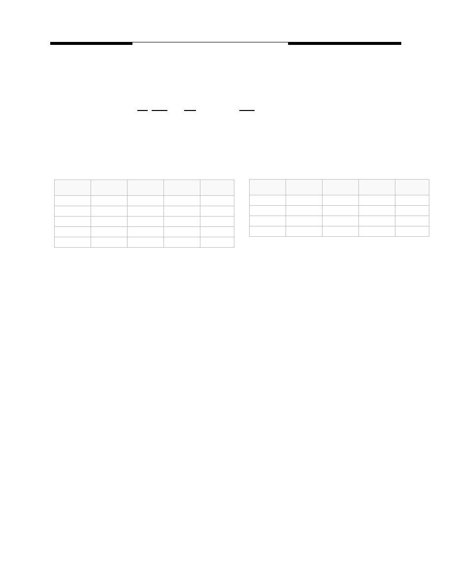
Bank Selection for Precharge by Address Bits
A10
BA0
BA1
Precharge
Bank(s)
LOW
Bank 0 only
LOW
HIGH
Bank 1 only
LOW
HIGH
LOW
Bank 2 only
LOW
HIGH
Bank 3 only
BA2
LOW
HIGH
LOW
Bank 4 only
A10
BA0
BA1
Precharge
Bank(s)
LOW
Bank 6 only
LOW
HIGH
Bank 7 only
All Banks
BA2
Bank 5 only
HIGH
LOW
HIGH
Don't Care
Burst Read Operation Followed by a Precharge
The following rules apply as long as the tRTP timing parameter - Internal Read to Precharge Command delay
time - is less or equal two clocks, which is the case for operating frequencies less or equal 266 Mhz (DDR2
400 and 533 speed sorts):
Minimum Read to Precharge command spacing to the same bank = AL + BL/2 clocks. For the earliest possi-
ble precharge, the precharge command may be issued on the rising edge which is “Additive Latency (AL) +
BL/2 clocks” after a Read Command, as long as the minimum tRAS timing is satisfied.
A new bank active command may be issued to the same bank if the following two conditions are satisfied
simultaneously:
(1) The RAS precharge time (tRP) has been satisfied from the clock at which the precharge begins.
(2) The RAS cycle time (tRCmin) from the previous bank activation has been satisfied.
For operating frequencies higher than 266 MHz, tRTP becomes > 2 clocks and one additional clock cycle
has to be added for the minimum Read to Precharge command spacing, which now becomes AL + BL/2 + 1
clocks.
相关PDF资料 |
PDF描述 |
|---|---|
| V59C1G01808QALF37E | 128M X 8 DDR DRAM, BGA68 |
| V59C1G01808QAUF37H | 128M X 8 DDR DRAM, PBGA68 |
| V59C1512804QALP19A | 64M X 8 DDR DRAM, PBGA68 |
| V59C1512804QAUF19AI | 64M X 8 DDR DRAM, PBGA68 |
| V59C1512804QAUP19AH | 64M X 8 DDR DRAM, PBGA68 |
相关代理商/技术参数 |
参数描述 |
|---|---|
| V5A010CB | 制造商:Honeywell Sensing and Control 功能描述:MICROSWITCH V5 PIN PLUNGER |
| V5A010CB | 制造商:Honeywell Sensing and Control 功能描述:MICROSWITCH V5 PIN PLUNGER |
| V5A010CB4D | 制造商:Honeywell Sensing and Control 功能描述:MICROSWITCH V5 ROLLER LEVER |
| V5A010CB4D | 制造商:Honeywell Sensing and Control 功能描述:MICROSWITCH V5 ROLLER LEVER |
| V5A010CB4E | 制造商:Honeywell Sensing and Control 功能描述:MICROSWITCH V5 ROLLER LEVER |
发布紧急采购,3分钟左右您将得到回复。