- 您现在的位置:买卖IC网 > PDF目录202173 > V59C1G01808QALF19E (PROMOS TECHNOLOGIES INC) 128M X 8 DDR DRAM, BGA68 PDF资料下载
参数资料
| 型号: | V59C1G01808QALF19E |
| 厂商: | PROMOS TECHNOLOGIES INC |
| 元件分类: | DRAM |
| 英文描述: | 128M X 8 DDR DRAM, BGA68 |
| 封装: | ROHS COMPLIANT, FBGA-68 |
| 文件页数: | 74/79页 |
| 文件大小: | 1028K |
| 代理商: | V59C1G01808QALF19E |
第1页第2页第3页第4页第5页第6页第7页第8页第9页第10页第11页第12页第13页第14页第15页第16页第17页第18页第19页第20页第21页第22页第23页第24页第25页第26页第27页第28页第29页第30页第31页第32页第33页第34页第35页第36页第37页第38页第39页第40页第41页第42页第43页第44页第45页第46页第47页第48页第49页第50页第51页第52页第53页第54页第55页第56页第57页第58页第59页第60页第61页第62页第63页第64页第65页第66页第67页第68页第69页第70页第71页第72页第73页当前第74页第75页第76页第77页第78页第79页
76
V59C1G01(408/808/168)QA Rev. 1.3 June 2008
ProMOS TECHNOLOGIES
V59C1G01(408/808/168)QA
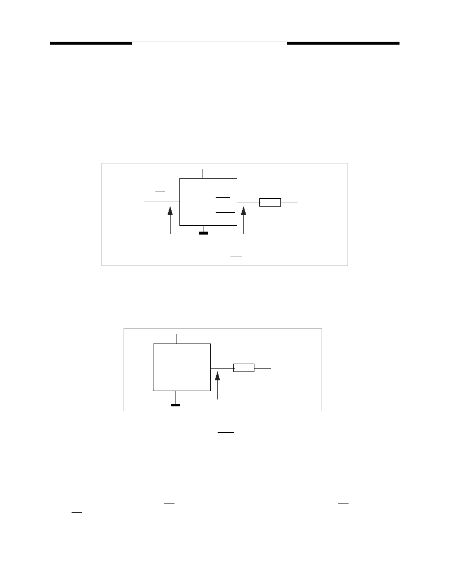
Reference Loads, Slew Rates and Slew Rate Derating
Reference Load for Timing Measurements
The figure represents the timing reference load used in defining the relevant timing parameters of the device.
It is not intended to either a precise representation of the typical system environment nor a depiction of the
actual load presented by a production tester. System designers will use IBIS or other simulation tools to cor-
relate the timing reference load to a system environment. This load circuit is also used for output slew rate
measurements.
25 Ohm
Vtt = VDDQ / 2
CK, CK
DUT
Timing Reference Points
VDDQ
DQ
DQS
RDQS
Note: The output timing reference voltage level for single ended signals is the crosspoint with VTT.
The output timing reference voltage level for differential signals is the crosspoint of the
true (e.g. DQS) and the complement (e.g. DQS) signal.
Slew Rate Measurements
Output Slew Rate
Output slew rate is characterized under the test conditions as shown in the figure below
25 Ohm
Vtt = VDDQ / 2
DUT
Test Point
VDDQ
DQ
DQS
RDQS
Output slew rate for falling and rising edges is measured between VTT - 250 mV and VTT + 250 mV for single
ended signals.For differential signals (e.g. DQS - DQS) output slew rate is measured between DQS - DQS =
- 500 mV and DQS - DQS = + 500 mV.Output slew rate is guaranteed by design, but is not necessarilty tested
on each device.
Input Slew Rate
Input slew for single ended signals is measured from dc-level to ac-level from VREF to VIH(AC),min for rising
and from VREF to VIL(AC), min or falling edges.
For differential signals (e.g. CK - CK) slew rate for rising edges is measured from CK - CK = -250 mV to
CK -CK = +500 mV (250 mV to -500 mV for falling edges). Test conditions are the same as for timing mea-
surements.
相关PDF资料 |
PDF描述 |
|---|---|
| V59C1G01808QALF37E | 128M X 8 DDR DRAM, BGA68 |
| V59C1G01808QAUF37H | 128M X 8 DDR DRAM, PBGA68 |
| V59C1512804QALP19A | 64M X 8 DDR DRAM, PBGA68 |
| V59C1512804QAUF19AI | 64M X 8 DDR DRAM, PBGA68 |
| V59C1512804QAUP19AH | 64M X 8 DDR DRAM, PBGA68 |
相关代理商/技术参数 |
参数描述 |
|---|---|
| V5A010CB | 制造商:Honeywell Sensing and Control 功能描述:MICROSWITCH V5 PIN PLUNGER |
| V5A010CB | 制造商:Honeywell Sensing and Control 功能描述:MICROSWITCH V5 PIN PLUNGER |
| V5A010CB4D | 制造商:Honeywell Sensing and Control 功能描述:MICROSWITCH V5 ROLLER LEVER |
| V5A010CB4D | 制造商:Honeywell Sensing and Control 功能描述:MICROSWITCH V5 ROLLER LEVER |
| V5A010CB4E | 制造商:Honeywell Sensing and Control 功能描述:MICROSWITCH V5 ROLLER LEVER |
发布紧急采购,3分钟左右您将得到回复。