- 您现在的位置:买卖IC网 > PDF目录202173 > V59C1G01808QALF19E (PROMOS TECHNOLOGIES INC) 128M X 8 DDR DRAM, BGA68 PDF资料下载
参数资料
| 型号: | V59C1G01808QALF19E |
| 厂商: | PROMOS TECHNOLOGIES INC |
| 元件分类: | DRAM |
| 英文描述: | 128M X 8 DDR DRAM, BGA68 |
| 封装: | ROHS COMPLIANT, FBGA-68 |
| 文件页数: | 60/79页 |
| 文件大小: | 1028K |
| 代理商: | V59C1G01808QALF19E |
第1页第2页第3页第4页第5页第6页第7页第8页第9页第10页第11页第12页第13页第14页第15页第16页第17页第18页第19页第20页第21页第22页第23页第24页第25页第26页第27页第28页第29页第30页第31页第32页第33页第34页第35页第36页第37页第38页第39页第40页第41页第42页第43页第44页第45页第46页第47页第48页第49页第50页第51页第52页第53页第54页第55页第56页第57页第58页第59页当前第60页第61页第62页第63页第64页第65页第66页第67页第68页第69页第70页第71页第72页第73页第74页第75页第76页第77页第78页第79页
63
ProMOS TECHNOLOGIES
V59C1G01(408/808/168)QA
V59C1G01(408/808/168)QA Rev. 1.3 June 2008
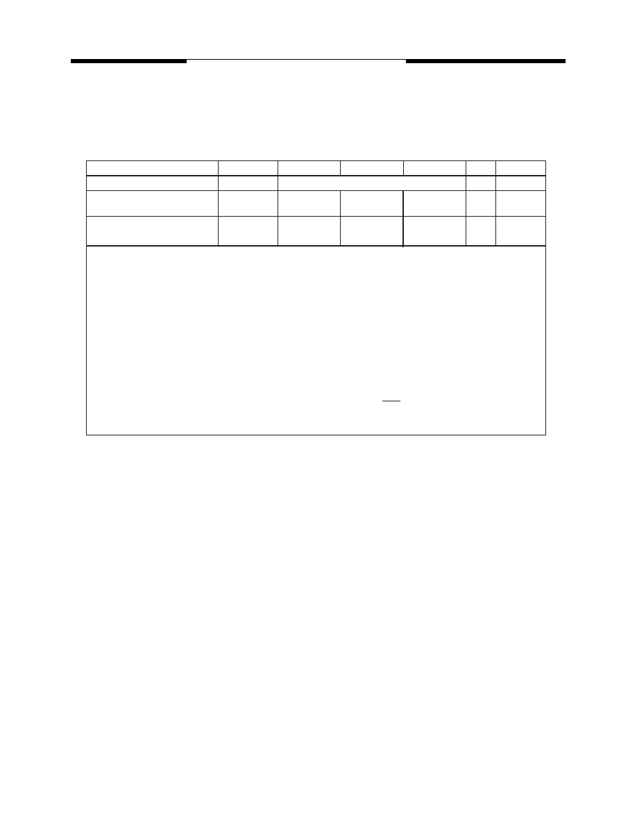
OCD de fault characteristics
Description
Parameter
Min
Nom
Max
Unit
Notes
Output impedance
See full strength default driver characteristics
1
Output impedance step size for
OCD calibration
0.5
6
Pull-up and pull-down mismatch
0
4
1,2,3
Output slew rate
Sout
1.5
5
V/ns
1,4,5,7,8,9
NOTE 1
Absolute Specifications (TOPER; VDD = +1.8V ±0.1V, VDDQ = +1.8V ±0.1V). DRAM I/O specifications for timing,
voltage, and slew rate are no longer applicable if OCD is changed from default settings.
NOTE 2
Impedance measurement condition for output source dc current: VDDQ = 1.7 V; VOUT = 1420 mV; (VOUT-
VDDQ)/Ioh must be less than 23.4
for values of VOUT between VDDQ and VDDQ - 280 mV. Impedance measurement condi-
tion for output sink dc current: VDDQ = 1.7 V; VOUT = 280 mV; VOUT/Iol must be less than 23.4
for values of VOUT
between 0 V and 280 mV.
NOTE 3
Mismatch is absolute value between pull-up and pull-down, both are measured at same temperature and voltage.
NOTE 4
Slew rate measured from vil(ac) to vih(ac).
NOTE 5
The absolute value of the slew rate as measured from DC to DC is equal to or greater than the slew rate as measured
from AC to AC. This is guaranteed by design and characterization.
NOTE 6
This represents the step size when the OCD is near 18
at nominal conditions across all process corners/variations
and represents only the DRAM uncertainty. A 0
value (no calibration) can only be achieved if the OCD impedance is 18
+/-
0.75
under nominal conditions.
NOTE 7
DRAM output slew rate specification applies to 667 MT/s speed bins.
NOTE 8
Timing skew due to DRAM output slew rate mis-match between DQS / DQS and associated DQ’s is included in
tDQSQ and tQHS specification.
NOTE 9
DDR2 SDRAM output slew rate test load is defined in General Note 3 of the AC Timing specification Table.
AC & DC operating conditions (cont'd)
相关PDF资料 |
PDF描述 |
|---|---|
| V59C1G01808QALF37E | 128M X 8 DDR DRAM, BGA68 |
| V59C1G01808QAUF37H | 128M X 8 DDR DRAM, PBGA68 |
| V59C1512804QALP19A | 64M X 8 DDR DRAM, PBGA68 |
| V59C1512804QAUF19AI | 64M X 8 DDR DRAM, PBGA68 |
| V59C1512804QAUP19AH | 64M X 8 DDR DRAM, PBGA68 |
相关代理商/技术参数 |
参数描述 |
|---|---|
| V5A010CB | 制造商:Honeywell Sensing and Control 功能描述:MICROSWITCH V5 PIN PLUNGER |
| V5A010CB | 制造商:Honeywell Sensing and Control 功能描述:MICROSWITCH V5 PIN PLUNGER |
| V5A010CB4D | 制造商:Honeywell Sensing and Control 功能描述:MICROSWITCH V5 ROLLER LEVER |
| V5A010CB4D | 制造商:Honeywell Sensing and Control 功能描述:MICROSWITCH V5 ROLLER LEVER |
| V5A010CB4E | 制造商:Honeywell Sensing and Control 功能描述:MICROSWITCH V5 ROLLER LEVER |
发布紧急采购,3分钟左右您将得到回复。