- 您现在的位置:买卖IC网 > PDF目录189259 > NT5CB256M4AN-BF (NANYA TECHNOLOGY CORP) DDR DRAM, PBGA78 PDF资料下载
参数资料
| 型号: | NT5CB256M4AN-BF |
| 厂商: | NANYA TECHNOLOGY CORP |
| 元件分类: | DRAM |
| 英文描述: | DDR DRAM, PBGA78 |
| 封装: | 0.80 MM PITCH, ROHS COMPLIANAT, WBGA-78 |
| 文件页数: | 34/106页 |
| 文件大小: | 2599K |
| 代理商: | NT5CB256M4AN-BF |
第1页第2页第3页第4页第5页第6页第7页第8页第9页第10页第11页第12页第13页第14页第15页第16页第17页第18页第19页第20页第21页第22页第23页第24页第25页第26页第27页第28页第29页第30页第31页第32页第33页当前第34页第35页第36页第37页第38页第39页第40页第41页第42页第43页第44页第45页第46页第47页第48页第49页第50页第51页第52页第53页第54页第55页第56页第57页第58页第59页第60页第61页第62页第63页第64页第65页第66页第67页第68页第69页第70页第71页第72页第73页第74页第75页第76页第77页第78页第79页第80页第81页第82页第83页第84页第85页第86页第87页第88页第89页第90页第91页第92页第93页第94页第95页第96页第97页第98页第99页第100页第101页第102页第103页第104页第105页第106页
1Gb DDR3 SDRAM A-Die
NT5CB256M4AN / NT5CB128M8AN / NT5CB64M16AP
33
REV 1.2
01 / 2009
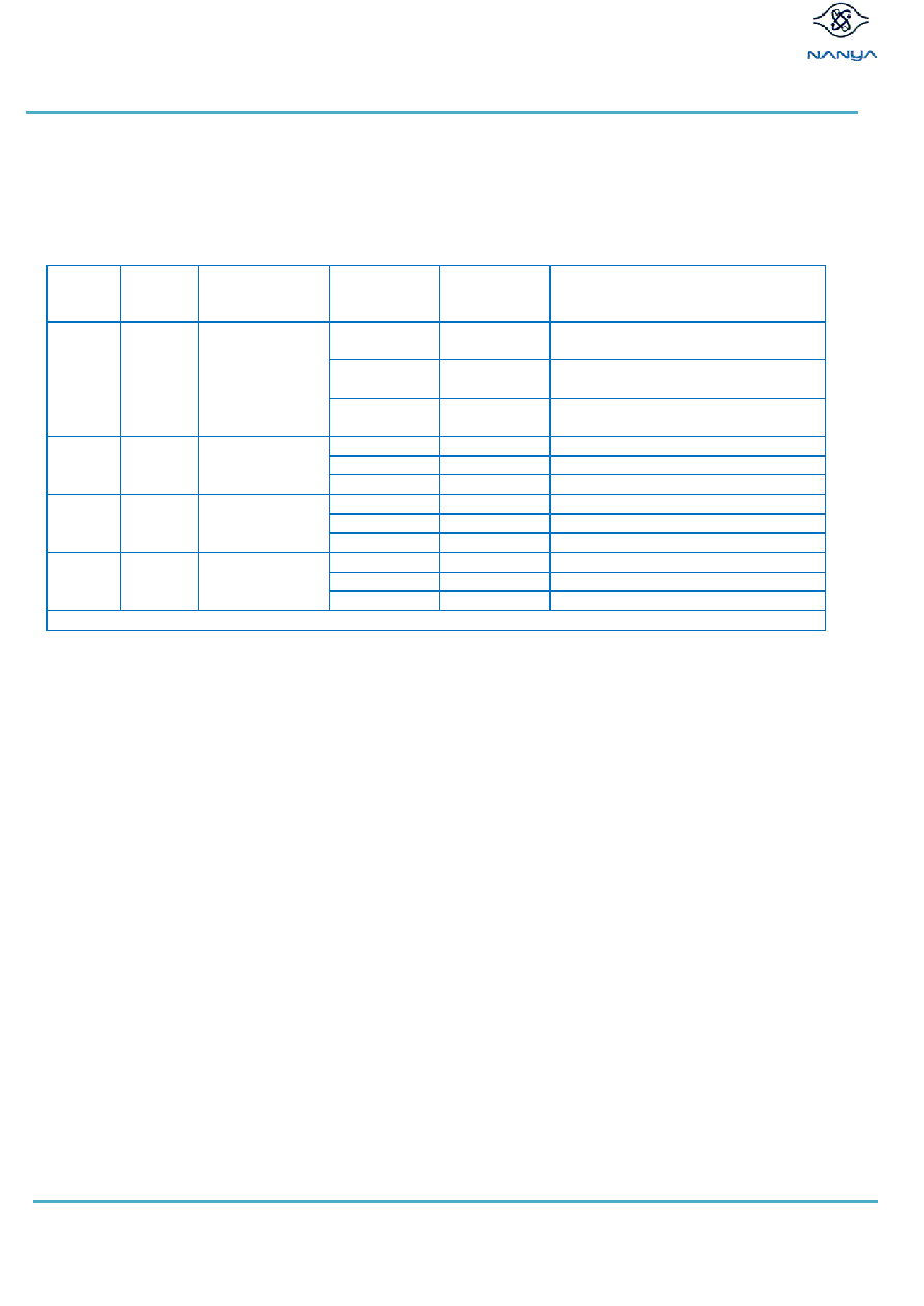
MPR Register Address Definition
The following table provide an overview of the available data location, how they are addressed by MR3 A[1:0] during a MRS to MR3,
and how their individual bits are mapped into the burst order bits during a Multi Purpose Register Read.
MPR MR3 Register Definition
MR3
A[2]
MR3
A[1:0]
Function
Burst Length
Read
Address
A[2:0]
Burst Order and Data Pattern
1
00
Read Predefined
Pattern for System
Calibration
BL8
000
Burst order 0,1,2,3,4,5,6,7
Pre-defined Data Pattern [0,1,0,1,0,1,0,1]
BC4
000
Burst order 0,1,2,3
Pre-defined Data Pattern [0,1,0,1]
BC4
100
Burst order 4,5,6,7
Pre-defined Data Pattern [0,1,0,1]
1
01
RFU
BL8
000
Burst order 0,1,2,3,4,5,6,7
BC4
000
Burst order 0,1,2,3
BC4
100
Burst order 4,5,6,7
1
10
RFU
BL8
000
Burst order 0,1,2,3,4,5,6,7
BC4
000
Burst order 0,1,2,3
BC4
100
Burst order 4,5,6,7
1
11
RFU
BL8
000
Burst order 0,1,2,3,4,5,6,7
BC4
000
Burst order 0,1,2,3
BC4
100
Burst order 4,5,6,7
Note: Burst order bit 0 is assigned to LSB and the burst order bit 7 is assigned to MSB of the selected MPR agent.
ACTIVE Command
The ACTIVE command is used to open (or activate) a row in a particular bank for subsequent access. The value on the BA0-BA2
inputs selects the bank, and the addresses provided on inputs A0-A13 selects the row. These rows remain active (or open) for
accesses until a precharge command is issued to that bank. A PRECHARGE command must be issued before opening a different row
in the same bank.
PRECHARGE Command
The PRECHARGE command is used to deactivate the open row in a particular bank or the open row in all banks. The bank(s) will be
available for a subsequent row activation a specified time (tRP) after the PRECHARGE command is issued, except in the case of
concurrent auto precharge, where a READ or WRITE command to a different bank is allowed as long as it does not interrupt the data
transfer in the current bank and does not violate any other timing parameters. Once a bank has been precharged, it is in the idle state
and must be activated prior to any READ or WRITE commands being issued to that bank. A PRECHARGE command is allowed if
there is no open row in that bank (idle bank) or if the previously open row is already in the process of precharging. However, the
precharge period will be determined by the last PRECHARGE command issued to the bank.
相关PDF资料 |
PDF描述 |
|---|---|
| NT5DS64M8BF-6KI | DDR DRAM, PBGA60 |
| NT5SE8M16DS-6K | 8M X 16 SYNCHRONOUS DRAM, 5 ns, PDSO54 |
| NT5SV8M8DT-7 | 8M X 8 SYNCHRONOUS DRAM, 5.4 ns, PDSO54 |
| NTC1111-20MHZ | Analog IC |
| NTC1111-SERIES | Analog IC |
相关代理商/技术参数 |
参数描述 |
|---|---|
| NT5CB256M8FN-DI | 制造商:Nanya Technology Corporation 功能描述:MEMORY IC |
| NT5CB256M8GN-CG | 制造商:Nanya Technology Corporation 功能描述:DRAM |
| NT5CB64M16DP-CF | 制造商:Nanya Technology Corporation 功能描述:DRAM |
| NT5CB64M16FP-DH | 制造商:Nanya Technology Corporation 功能描述:MEMORY |
| NT5CB64M16FP-DII | 制造商:Nanya Technology Corporation 功能描述:MEMORY IC |
发布紧急采购,3分钟左右您将得到回复。