- 您现在的位置:买卖IC网 > PDF目录4580 > IDT88P8341BHGI (IDT, Integrated Device Technology Inc)IC SPI3-SPI4 EXCHANGE 820-PBGA PDF资料下载
参数资料
| 型号: | IDT88P8341BHGI |
| 厂商: | IDT, Integrated Device Technology Inc |
| 文件页数: | 53/96页 |
| 文件大小: | 0K |
| 描述: | IC SPI3-SPI4 EXCHANGE 820-PBGA |
| 标准包装: | 24 |
| 系列: | * |
| 其它名称: | 88P8341BHGI |
第1页第2页第3页第4页第5页第6页第7页第8页第9页第10页第11页第12页第13页第14页第15页第16页第17页第18页第19页第20页第21页第22页第23页第24页第25页第26页第27页第28页第29页第30页第31页第32页第33页第34页第35页第36页第37页第38页第39页第40页第41页第42页第43页第44页第45页第46页第47页第48页第49页第50页第51页第52页当前第53页第54页第55页第56页第57页第58页第59页第60页第61页第62页第63页第64页第65页第66页第67页第68页第69页第70页第71页第72页第73页第74页第75页第76页第77页第78页第79页第80页第81页第82页第83页第84页第85页第86页第87页第88页第89页第90页第91页第92页第93页第94页第95页第96页
57
IDT88P8341 SPI EXCHANGE SPI-3 TO SPI-4
INDUSTRIALTEMPERATURERANGE
APRIL 10, 2006
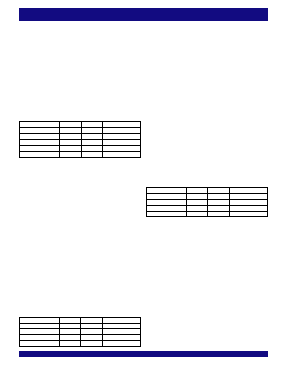
TABLE 56 - SPI-4 INGRESS TO SPI-3 EGRESS FLOW
CONTROLREGISTER(REGISTER_OFFSET=0x01)
Field
Bits
Length
Initial Value
CREDIT_EN
0
1
0b0
BURST_EN
1
0b0
LOOP_BACK
2
1
0b0
Reserved
31:3
29
0x00
TABLE 57 - SPI-3 EGRESS TEST REGISTER
(REGISTER_OFFSET=0x02)
Field
Bits
Length
Initial Value
ADD_PAR_ERR
0
1
0b0
DAT_PAR_ERR
1
0b0
Reserved
7:2
6
0x00
PORT_ADDRESS
15:8
8
0x0F
ENABLE
This bit is used to enable or disable the connection of a LID to
an LP.
0=LP disabled
1=LP enabled
BIT_REVERSAL This bit is used to reverse the bit ordering of each byte
of the SPI-3 interface on a per-LP basis.
0=Disable bit reversal for an LP
1=Enable bit reversal for an LP
9.3.4 Block base 0x0700 registers
SPI-3 egress configuration register (Block_base
0x0700 + Register_offset 0x00)
There is one SPI-3 egress configuration register per SPI-3 interface. The
SPI-3 egress configuration registers have read and write access. A SPI-3
egress configuration registers is used to control the poll sequence length of a
SPI-3 egress interface when the SPI-3 interface is in Link mode. The SPI-3
egress configuration register is used to add two cycles to STX or EOP as
required to interface to the attached device.
POLL_LENGTH Link layer poll sequence length when in Link mode. The
pollsequenceisfromtheLPassociatedwithLID0totheLPassociatedwiththe
LID for POLL_LENGTH - 1.
STX_SPACING This bit is used to enable or disable the adding of two
dummySTXcyclestotheSPI-3egressinterfacetomeettheneedsofanattached
device.
0= No dummy STX cycles are added to the SPI-3 egress.
1= Two dummy STX cycles are added to the SPI-3 egress
EOP_SPACING This bit is used to enable or disable the adding of two
dummyEOPcyclestotheSPI-3egressinterfacetomeettheneedsofanattached
device.
0= No dummy EOP cycles are added to the SPI-3 egress.
1= Two dummy EOP cycles are added to the SPI-3 egress
SPI-4 ingress to SPI-3 egress flow control register
(Block_base 0x0700 + Register_offset 0x01)
The SPI-4 ingress to SPI-3 egress flow control register has read and write
access. The bit fields of the SPI-4 ingress to SPI-3 egress flow control register
are described.
CREDIT_EN
CREDIT_EN Theflowcontrolinformationreceivedfrom
theattachedSPI-3deviceisinterpretedasstatusorcreditinformationasselected
bytheCREDIT_ENbitintheSPI-4ingresstoSPI-3egressflowcontrolRegister.
If the status mode is used, data will be egressed until the status is changed by
the attached SPI-3 device. If the credit mode is used, the SPI-3 egress will
transmitonlyonepacketfragmentandthenwaitforanupdateintheinternalbuffer
segment pool status before sending another packet fragment.
0=Statusmode
1=Credit mode
BURST_EN
MultipleBurstEnableallowsmorethanonebursttobesent
to an LP. When this feature is not enabled, only one burst per LP is allowed into
the SPI-3 egress buffers.
0=Disable burst enable
1=Enable burst enable
LOOP_BACK
In this mode the contents of a SPI-3 ingress are directly
transferred to a SPI-3 egress buffers of the same port. This mode is useful for
off-linediagnostics.
0=Disable loopback
1=Enable loopback
SPI-3 egress test register (Block_base 0x0700 +
Register_offset 0x02)
TABLE 55 - SPI-3 EGRESS CONFIGURATION
REGISTER(REGISTER_OFFSET=0x00)
Field
Bits
Length
Initial Value
POLL_LENGTH
5:0
6
0x0F
Reserved
7:6
2
0b00
STX_SPACING
8
1
0b0
EOP_SPACING
9
1
0b0
Reserved
31:10
22
0x00
The SPI-3 egress test register has read and write access. A single address
parity error is introduced on the SPI-3 egress LP through the ADD_PAR_ERR
bit field. A single data parity error is introduced on the SPI-3 egress LP through
the DAT_PAR_ERR bit field. The LP affected by these two parity error bit fields
isenumeratedinthePORT_ADDRESSfield.ThebitfieldsofSPI-3egresstest
register are described. The bit fields are automatically cleared following the
generation of the associated error.
ADD_PAR_ERR
A single address parity error is introduced on the SPI-
3 egress LP through the ADD_PAR_ERR bit field. The LP affected by the
ADD_PAR_ERR bit field is enumerated in the PORT_ADDRESS field.
0=No parity error introduced
1=Introduce a single address parity error on the SPI-3 egress LP
DAT_PAR_ERR
A single data parity error is introduced on the SPI-3
egress LP through the DAT_PAR_ERR bit field. The LP affected by the
DAT_PAR_ERR bit field is enumerated in the PORT_ADDRESS field.
0=No parity error introduced
1=Introduce a single data parity error on the SPI-3 egress LP
PORT_ADDRESS
The LP affected by both the ADD_PAR_ERR
andtheDAT_PAR_ERRbitfieldsisenumeratedinthePORT_ADDRESSfield.
The value of the PORT_ADDRESS is set from 0x00 to 0xFF.
相关PDF资料 |
PDF描述 |
|---|---|
| LFEC15E-4FN484C | IC FPGA 10.2KLUTS 288I/O 484-BGA |
| IDT72V51446L7-5BBI | IC FLOW CTRL MULTI QUEUE 256-BGA |
| LFEC15E-4F484C | IC FPGA 10.2KLUTS 288I/O 484-BGA |
| LT3022IMSE-1.8#TRPBF | IC REG LDO 1.8V 1A 16-MSOP |
| LT3022IMSE-1.5#TRPBF | IC REG LDO 1.5V 1A 16-MSOP |
相关代理商/技术参数 |
参数描述 |
|---|---|
| IDT88P8341BHI | 功能描述:IC SPI3-SPI4 EXCHANGE 820-PBGA RoHS:否 类别:集成电路 (IC) >> 专用 IC 系列:* 产品培训模块:Lead (SnPb) Finish for COTS Obsolescence Mitigation Program 标准包装:1 系列:- 类型:调帧器 应用:数据传输 安装类型:表面贴装 封装/外壳:400-BBGA 供应商设备封装:400-PBGA(27x27) 包装:散装 |
| IDT88P8342BHGI | 功能描述:IC SPI3-SPI4 EXCHANGE 820-PBGA RoHS:是 类别:集成电路 (IC) >> 专用 IC 系列:* 产品培训模块:Lead (SnPb) Finish for COTS Obsolescence Mitigation Program 标准包装:1 系列:- 类型:调帧器 应用:数据传输 安装类型:表面贴装 封装/外壳:400-BBGA 供应商设备封装:400-PBGA(27x27) 包装:散装 |
| IDT88P8342BHI | 功能描述:IC SPI3-SPI4 EXCHANGE 820-PBGA RoHS:否 类别:集成电路 (IC) >> 专用 IC 系列:* 产品培训模块:Lead (SnPb) Finish for COTS Obsolescence Mitigation Program 标准包装:1 系列:- 类型:调帧器 应用:数据传输 安装类型:表面贴装 封装/外壳:400-BBGA 供应商设备封装:400-PBGA(27x27) 包装:散装 |
| IDT88P8344 | 制造商:IDT 制造商全称:Integrated Device Technology 功能描述:SPI EXCHANGE 4 x SPI-3 TO SPI-4 Issue 1.0 |
| IDT88P8344BHGI | 功能描述:IC SPI3-SPI4 EXCHANGE 820-PBGA RoHS:是 类别:集成电路 (IC) >> 专用 IC 系列:* 产品培训模块:Lead (SnPb) Finish for COTS Obsolescence Mitigation Program 标准包装:1 系列:- 类型:调帧器 应用:数据传输 安装类型:表面贴装 封装/外壳:400-BBGA 供应商设备封装:400-PBGA(27x27) 包装:散装 |
发布紧急采购,3分钟左右您将得到回复。