- 您现在的位置:买卖IC网 > PDF目录4101 > MT42L64M32D1KL-3 IT:A (Micron Technology Inc)IC DDR2 SDRAM 2GBIT 168FBGA PDF资料下载
参数资料
| 型号: | MT42L64M32D1KL-3 IT:A |
| 厂商: | Micron Technology Inc |
| 文件页数: | 91/164页 |
| 文件大小: | 0K |
| 描述: | IC DDR2 SDRAM 2GBIT 168FBGA |
| 标准包装: | 1,000 |
| 格式 - 存储器: | RAM |
| 存储器类型: | 移动 LPDDR2 SDRAM |
| 存储容量: | 2G(64M x 32) |
| 速度: | 333MHz |
| 接口: | 并联 |
| 电源电压: | 1.14 V ~ 1.3 V |
| 工作温度: | -25°C ~ 85°C |
| 封装/外壳: | 168-WFBGA |
| 供应商设备封装: | 168-FBGA(12x12) |
| 包装: | 散装 |
第1页第2页第3页第4页第5页第6页第7页第8页第9页第10页第11页第12页第13页第14页第15页第16页第17页第18页第19页第20页第21页第22页第23页第24页第25页第26页第27页第28页第29页第30页第31页第32页第33页第34页第35页第36页第37页第38页第39页第40页第41页第42页第43页第44页第45页第46页第47页第48页第49页第50页第51页第52页第53页第54页第55页第56页第57页第58页第59页第60页第61页第62页第63页第64页第65页第66页第67页第68页第69页第70页第71页第72页第73页第74页第75页第76页第77页第78页第79页第80页第81页第82页第83页第84页第85页第86页第87页第88页第89页第90页当前第91页第92页第93页第94页第95页第96页第97页第98页第99页第100页第101页第102页第103页第104页第105页第106页第107页第108页第109页第110页第111页第112页第113页第114页第115页第116页第117页第118页第119页第120页第121页第122页第123页第124页第125页第126页第127页第128页第129页第130页第131页第132页第133页第134页第135页第136页第137页第138页第139页第140页第141页第142页第143页第144页第145页第146页第147页第148页第149页第150页第151页第152页第153页第154页第155页第156页第157页第158页第159页第160页第161页第162页第163页第164页
�� �
�
�2Gb:� x16,� x32� Mobile� LPDDR2� SDRAM� S4�
�MODE� REGISTER� WRITE� Command�
�MODE� REGISTER� WRITE� Command�
�The� MODE� REGISTER� WRITE� (MRW)� command� is� used� to� write� configuration� data� to�
�the� mode� registers.� The� MRW� command� is� initiated� with� CS#� LOW,� CA0� LOW,� CA1� LOW,�
�CA2� LOW,� and� CA3� LOW� at� the� rising� edge� of� the� clock.� The� mode� register� is� selected� by�
�CA1f–CA0f,� CA9r–CA4r.� The� data� to� be� written� to� the� mode� register� is� contained� in�
�CA9f–CA2f.� The� MRW� command� period� is� defined� by� t� MRW.� MRWs� to� read-only� regis-�
�ters� have� no� impact� on� the� functionality� of� the� device.�
�MRW� can� only� be� issued� when� all� banks� are� in� the� idle� precharge� state.� One� method� of�
�ensuring� that� the� banks� are� in� this� state� is� to� issue� a� PRECHARGE� ALL� command.�
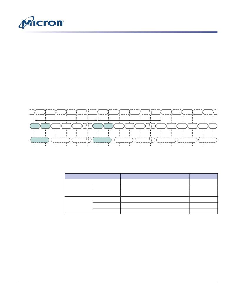
�Figure� 66:� MODE� REGISTER� WRITE� Timing� –� RL� =� 3,� t� MRW� =� 5�
�T0�
�T1�
�T2�
�Tx�
�Tx� +� 1�
�Tx� +� 2�
�Ty� 1�
�Ty� +� 1�
�Ty� +� 2�
�CK#�
�CK�
�t� MRW�
�t� MRW�
�CA[9:0]�
�MR� addr� MR� data�
�MR� addr� MR� data�
�CMD�
�MRW�
�NOP� 2�
�NOP� 2�
�MRW�
�NOP� 2�
�NOP� 2�
�Valid�
�Notes:�
�1.� At� time� Ty,� the� device� is� in� the� idle� state.�
�2.� Only� the� NOP� command� is� supported� during� t� MRW.�
�Table� 48:� Truth� Table� for� MRR� and� MRW�
�Current� State�
�All� banks� idle�
�Bank(s)� active�
�Command�
�MRR�
�MRW�
�MRW� (RESET)�
�MRR�
�MRW�
�MRW� (RESET)�
�Intermediate� State�
�Reading� mode� register,� all� banks� idle�
�Writing� mode� register,� all� banks� idle�
�Resetting,� device� auto� initialization�
�Reading� mode� register,� bank(s)� idle�
�Not� allowed�
�Not� allowed�
�Next� State�
�All� banks� idle�
�All� banks� idle�
�All� banks� idle�
�Bank(s)� active�
�Not� allowed�
�Not� allowed�
�MRW� RESET� Command�
�The� MRW� RESET� command� brings� the� device� to� the� device� auto� initialization� (reset-�
�ting)� state� in� the� power-on� initialization� sequence� (see� 2.� RESET� Command� under� Pow-�
�er-Up� (page� 40)).� The� MRW� RESET� command� can� be� issued� from� the� idle� state.� This�
�command� resets� all� mode� registers� to� their� default� values.� Only� the� NOP� command� is�
�supported� during� t� INIT4.� After� MRW� RESET,� boot� timings� must� be� observed� until� the�
�device� initialization� sequence� is� complete� and� the� device� is� in� the� idle� state.� Array� data�
�is� undefined� after� the� MRW� RESET� command� has� completed.�
�For� MRW� RESET� timing,� see� Figure� 26� (page� 42).�
�PDF:� 09005aef83f3f2eb�
�2gb_mobile_lpddr2_s4_g69a.pdf� –� Rev.� N� 3/12� EN�
�91�
�Micron� Technology,� Inc.� reserves� the� right� to� change� products� or� specifications� without� notice.�
�2010� Micron� Technology,� Inc.� All� rights� reserved.�
�相关PDF资料 |
PDF描述 |
|---|---|
| GSC60DTEI | CONN EDGECARD 120POS .100 EYELET |
| MT42L64M32D1KL-25 IT:A | IC DDR2 SDRAM 2GBIT 168FBGA |
| IDT71V67803S133BQG8 | IC SRAM 9MBIT 133MHZ 165FBGA |
| IDT71V65803S150PFG | IC SRAM 9MBIT 150MHZ 100TQFP |
| IDT71V67903S85BQI8 | IC SRAM 9MBIT 85NS 165FBGA |
相关代理商/技术参数 |
参数描述 |
|---|
发布紧急采购,3分钟左右您将得到回复。