- 您现在的位置:买卖IC网 > PDF目录11210 > ADUC7061BCPZ32-RL (Analog Devices Inc)IC MCU 16/32BIT 32KB 32LFCSP PDF资料下载
参数资料
| 型号: | ADUC7061BCPZ32-RL |
| 厂商: | Analog Devices Inc |
| 文件页数: | 16/108页 |
| 文件大小: | 0K |
| 描述: | IC MCU 16/32BIT 32KB 32LFCSP |
| 产品变化通告: | ADuC7060/1 Idd Specification Change 01/Feb/2010 |
| 设计资源: | USB Based Temperature Monitor Using ADuC7061 and an External RTD (CN0075) 4 mA-to-20 mA Loop-Powered Temperature Monitor Using ADuC7060/1 (CN0145) |
| 标准包装: | 5,000 |
| 系列: | MicroConverter® ADuC7xxx |
| 核心处理器: | ARM7 |
| 芯体尺寸: | 16/32-位 |
| 速度: | 10MHz |
| 连通性: | I²C,SPI,UART/USART |
| 外围设备: | POR,PWM,温度传感器,WDT |
| 输入/输出数: | 8 |
| 程序存储器容量: | 32KB(16K x 16) |
| 程序存储器类型: | 闪存 |
| RAM 容量: | 1K x 32 |
| 电压 - 电源 (Vcc/Vdd): | 2.375 V ~ 2.625 V |
| 数据转换器: | A/D 5x24b,8x24b,D/A 1x14b |
| 振荡器型: | 内部 |
| 工作温度: | -40°C ~ 125°C |
| 封装/外壳: | 32-VFQFN 裸露焊盘,CSP |
| 包装: | 带卷 (TR) |
第1页第2页第3页第4页第5页第6页第7页第8页第9页第10页第11页第12页第13页第14页第15页当前第16页第17页第18页第19页第20页第21页第22页第23页第24页第25页第26页第27页第28页第29页第30页第31页第32页第33页第34页第35页第36页第37页第38页第39页第40页第41页第42页第43页第44页第45页第46页第47页第48页第49页第50页第51页第52页第53页第54页第55页第56页第57页第58页第59页第60页第61页第62页第63页第64页第65页第66页第67页第68页第69页第70页第71页第72页第73页第74页第75页第76页第77页第78页第79页第80页第81页第82页第83页第84页第85页第86页第87页第88页第89页第90页第91页第92页第93页第94页第95页第96页第97页第98页第99页第100页第101页第102页第103页第104页第105页第106页第107页第108页
Data Sheet
ADuC7060/ADuC7061
Rev. D | Page 15 of 108
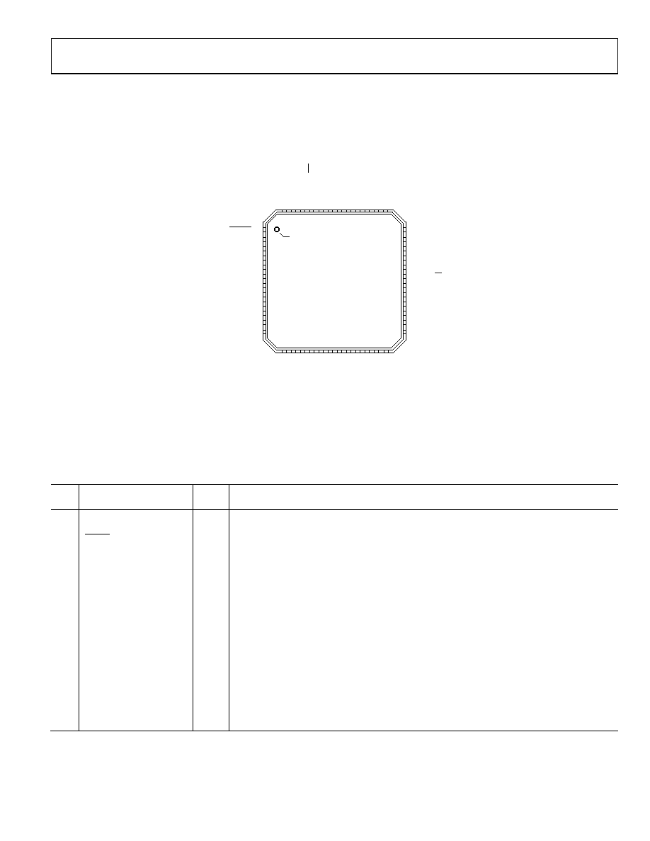
PIN CONFIGURATIONS AND FUNCTION DESCRIPTIONS
T
CK
T
DI
T
DO
DV
DD
DG
ND
P
2
.1
/IR
Q3
/P
WM
5
P1
.6
/PW
M4
P1
.5
/PW
M3
P1
.4
/PW
M2
P
2
.0
/IR
Q2
/P
WM
0
/E
X
TC
LK
P
0
.4
/IR
Q0
/P
WM
1
XTALO
P0.3/MOSI/SDA
P0.2/MISO
DVDD
P0.0/SS
P0.1/SCLK/SCL
XTALI
DGND
ADC9
ADC8
ADC6
ADC7
TMS
P1.0/IRQ1/SIN/T0
P1.1/SOUT
P0.5/CTS
P1.3/TRIP
P1.2/SYNC
P0.6/RTS
DVDD
DGND
ADC5/EXT_REF2IN
DAC0
ADC4/
E
X
T
_RE
F
2I
N+
ADC3
ADC2
IEXC
1
IEXC
0
G
ND_S
W
ADC1
ADC0
VR
EF
+
VR
EF
AG
ND
AV
DD
RESET
07079-
002
13
14
15
16
17
18
19
20
21
22
23
24
48
47
46
45
44
43
42
41
40
39
38
37
1
2
3
4
5
6
7
8
9
10
11
12
35
36
34
33
32
31
30
29
28
27
26
25
ADuC7060
TOP VIEW
(Not to Scale)
PIN 1
INDICATOR
NOTES
1. THE LFCSP_VQ ONLY HAS AN EXPOSED PADDLE THAT MUST BE LEFT UNCONNECTED.
THIS DOES NOT APPLY TO THE LQFP.
NT
RS
T
/BM
Figure 7. 48-Lead LQFP and 48-Lead LFCSP_VQ Pin Configuration
Table 8. ADuC7060 Pin Function Descriptions
Pin
No.
Mnemonic
Type1
Description
0
EP
Exposed Paddle. The LFCSP_VQ only has an exposed paddle that must be left unconnected.
This does not apply to the LQFP.
1
RESET
I
Reset. Input pin, active low. An external 1 k pull-up resistor is recommended with this pin.
2
TMS
I
JTAG Test Mode Select. Input pin used for debug and download. An external pull-up resistor
(~100 k) should be added to this pin.
3
P1.0/IRQ1/SIN/T0
I/O
General-Purpose Input and General Purpose Output P1.0/External Interrupt Request 1/Serial
Input/Timer0 Input. This is a multifunction input/output pin offering four functions.
4
P1.1/SOUT
I/O
General-Purpose Input and General-Purpose Output P1.1/Serial Output. This is a dual function
input/output pin.
5
P1.2/SYNC
I/O
General-Purpose Input and General-Purpose Output P1.2/PWM External Sync Input. This is a
dual function input/output pin.
6
P1.3/TRIP
I/O
General-Purpose Input and General-Purpose Output P1.3/PWM External Trip Input. This is a
dual function input/output pin.
7
P0.5/CTS
I/O
General-Purpose Input and General-Purpose Output P0.5/Clear-to-Send Signal in UART Mode.
8
P0.6/RTS
I/O
General-Purpose Input and General-Purpose Output P0.6/Request-to-Send Signal in UART Mode.
9
DVDD
S
Digital Supply Pin.
10
DGND
S
Digital Ground.
11
DAC0
O
DAC Output. Analog output pin.
相关PDF资料 |
PDF描述 |
|---|---|
| VI-B2L-IW-F4 | CONVERTER MOD DC/DC 28V 100W |
| ATMEGA8535L-8JU | MCU AVR 8K ISP FLASH MEM 44-PLCC |
| VI-B2L-IW-F3 | CONVERTER MOD DC/DC 28V 100W |
| ATMEGA8535L-8PU | IC AVR MCU 8K 8MHZ 3V 40DIP |
| VI-B2L-IW-F2 | CONVERTER MOD DC/DC 28V 100W |
相关代理商/技术参数 |
参数描述 |
|---|---|
| ADUC70SMARTLINKRL7 | 制造商:Analog Devices 功能描述: |
| ADUC70TEL | 制造商:Analog Devices 功能描述:FLASH ARM +5-CH 12BIT ADC - Trays |
| ADUC70TEL-RL7 | 制造商:Analog Devices 功能描述: |
| ADUC7120BBCZ | 制造商:Analog Devices 功能描述:- Rail/Tube |
| ADUC7120BBCZ-RL | 制造商:Analog Devices 功能描述:- Tape and Reel |
发布紧急采购,3分钟左右您将得到回复。