- 您现在的位置:买卖IC网 > PDF目录11210 > ADUC7061BCPZ32-RL (Analog Devices Inc)IC MCU 16/32BIT 32KB 32LFCSP PDF资料下载
参数资料
| 型号: | ADUC7061BCPZ32-RL |
| 厂商: | Analog Devices Inc |
| 文件页数: | 7/108页 |
| 文件大小: | 0K |
| 描述: | IC MCU 16/32BIT 32KB 32LFCSP |
| 产品变化通告: | ADuC7060/1 Idd Specification Change 01/Feb/2010 |
| 设计资源: | USB Based Temperature Monitor Using ADuC7061 and an External RTD (CN0075) 4 mA-to-20 mA Loop-Powered Temperature Monitor Using ADuC7060/1 (CN0145) |
| 标准包装: | 5,000 |
| 系列: | MicroConverter® ADuC7xxx |
| 核心处理器: | ARM7 |
| 芯体尺寸: | 16/32-位 |
| 速度: | 10MHz |
| 连通性: | I²C,SPI,UART/USART |
| 外围设备: | POR,PWM,温度传感器,WDT |
| 输入/输出数: | 8 |
| 程序存储器容量: | 32KB(16K x 16) |
| 程序存储器类型: | 闪存 |
| RAM 容量: | 1K x 32 |
| 电压 - 电源 (Vcc/Vdd): | 2.375 V ~ 2.625 V |
| 数据转换器: | A/D 5x24b,8x24b,D/A 1x14b |
| 振荡器型: | 内部 |
| 工作温度: | -40°C ~ 125°C |
| 封装/外壳: | 32-VFQFN 裸露焊盘,CSP |
| 包装: | 带卷 (TR) |
第1页第2页第3页第4页第5页第6页当前第7页第8页第9页第10页第11页第12页第13页第14页第15页第16页第17页第18页第19页第20页第21页第22页第23页第24页第25页第26页第27页第28页第29页第30页第31页第32页第33页第34页第35页第36页第37页第38页第39页第40页第41页第42页第43页第44页第45页第46页第47页第48页第49页第50页第51页第52页第53页第54页第55页第56页第57页第58页第59页第60页第61页第62页第63页第64页第65页第66页第67页第68页第69页第70页第71页第72页第73页第74页第75页第76页第77页第78页第79页第80页第81页第82页第83页第84页第85页第86页第87页第88页第89页第90页第91页第92页第93页第94页第95页第96页第97页第98页第99页第100页第101页第102页第103页第104页第105页第106页第107页第108页
ADuC7060/ADuC7061
Data Sheet
Rev. D | Page 104 of 108
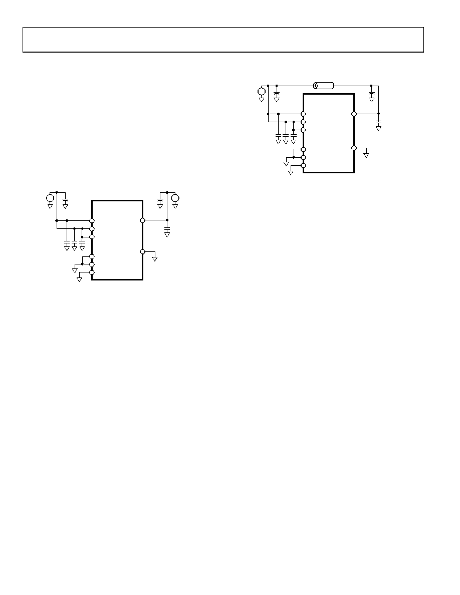
HARDWARE DESIGN CONSIDERATIONS
POWER SUPPLIES
The ADuC706x operational power supply voltage range is
2.375 V to 2.625 V. Separate analog and digital power supply
pins (AVDD and DVDD, respectively) allow AVDD to be kept
relatively free of noisy digital signals often present on the
system DVDD line. In this mode, the part can also operate with
split supplies; that is, it can use different voltage levels for each
supply. For example, the system can be designed to operate
with a DVDD voltage level of 2.6 V, whereas the AVDD level
can be at 2.5 V or vice versa. A typical split supply
configuration is shown in Figure 28.
ADuC7060/
ADuC7061
0.1F
ANALOG
SUPPLY
10F
AVDD
DVDD
DGND
AGND
0.1F
+
–
DIGITAL
SUPPLY
10F
+
–
07079-
022
Figure 28. External Dual Supply Connections
As an alternative to providing two separate power supplies, the
user can reduce noise on AVDD by placing a small series
resistor and/or ferrite bead between AVDD and DVDD, and then
decoupling AVDD separately to ground. An example of this
configuration is shown in Figure 29. With this configuration,
other analog circuitry (such as op amps, voltage reference, and
others) can be powered from the AVDD supply line as well.
ADuC7060/
ADuC7061
0.1F
ANALOG
SUPPLY
10F
AVDD
DVDD
DGND
AGND
0.1F
DIGITAL
SUPPLY
BEAD
10F
+
–
07079-
023
Figure 29. External Single Supply Connections
Notice that in both Figure 28 and Figure 29, a large value (10 F)
reservoir capacitor sits on DVDD, and a separate 10 F
capacitor sits on AVDD. In addition, local, small value (0.1 F)
capacitors are located at each AVDD and DVDD pin of the chip.
As per standard design practice, be sure to include all of these
capacitors and ensure that the smaller capacitors are close to the
AVDD pin with trace lengths as short as possible. Connect the
ground terminal of each of these capacitors directly to the
underlying ground plane.
Note that the analog and digital ground pins on the ADuC706x
must be referenced to the same system ground reference point
at all times.
Finally, note that, when the DVDD supply reaches 1.8 V, it must
ramp to 2.25 V in less than 128 ms. This is a requirement of the
internal power-on reset circuitry.
相关PDF资料 |
PDF描述 |
|---|---|
| VI-B2L-IW-F4 | CONVERTER MOD DC/DC 28V 100W |
| ATMEGA8535L-8JU | MCU AVR 8K ISP FLASH MEM 44-PLCC |
| VI-B2L-IW-F3 | CONVERTER MOD DC/DC 28V 100W |
| ATMEGA8535L-8PU | IC AVR MCU 8K 8MHZ 3V 40DIP |
| VI-B2L-IW-F2 | CONVERTER MOD DC/DC 28V 100W |
相关代理商/技术参数 |
参数描述 |
|---|---|
| ADUC70SMARTLINKRL7 | 制造商:Analog Devices 功能描述: |
| ADUC70TEL | 制造商:Analog Devices 功能描述:FLASH ARM +5-CH 12BIT ADC - Trays |
| ADUC70TEL-RL7 | 制造商:Analog Devices 功能描述: |
| ADUC7120BBCZ | 制造商:Analog Devices 功能描述:- Rail/Tube |
| ADUC7120BBCZ-RL | 制造商:Analog Devices 功能描述:- Tape and Reel |
发布紧急采购,3分钟左右您将得到回复。