- 您现在的位置:买卖IC网 > PDF目录11210 > ADUC7061BCPZ32-RL (Analog Devices Inc)IC MCU 16/32BIT 32KB 32LFCSP PDF资料下载
参数资料
| 型号: | ADUC7061BCPZ32-RL |
| 厂商: | Analog Devices Inc |
| 文件页数: | 82/108页 |
| 文件大小: | 0K |
| 描述: | IC MCU 16/32BIT 32KB 32LFCSP |
| 产品变化通告: | ADuC7060/1 Idd Specification Change 01/Feb/2010 |
| 设计资源: | USB Based Temperature Monitor Using ADuC7061 and an External RTD (CN0075) 4 mA-to-20 mA Loop-Powered Temperature Monitor Using ADuC7060/1 (CN0145) |
| 标准包装: | 5,000 |
| 系列: | MicroConverter® ADuC7xxx |
| 核心处理器: | ARM7 |
| 芯体尺寸: | 16/32-位 |
| 速度: | 10MHz |
| 连通性: | I²C,SPI,UART/USART |
| 外围设备: | POR,PWM,温度传感器,WDT |
| 输入/输出数: | 8 |
| 程序存储器容量: | 32KB(16K x 16) |
| 程序存储器类型: | 闪存 |
| RAM 容量: | 1K x 32 |
| 电压 - 电源 (Vcc/Vdd): | 2.375 V ~ 2.625 V |
| 数据转换器: | A/D 5x24b,8x24b,D/A 1x14b |
| 振荡器型: | 内部 |
| 工作温度: | -40°C ~ 125°C |
| 封装/外壳: | 32-VFQFN 裸露焊盘,CSP |
| 包装: | 带卷 (TR) |
第1页第2页第3页第4页第5页第6页第7页第8页第9页第10页第11页第12页第13页第14页第15页第16页第17页第18页第19页第20页第21页第22页第23页第24页第25页第26页第27页第28页第29页第30页第31页第32页第33页第34页第35页第36页第37页第38页第39页第40页第41页第42页第43页第44页第45页第46页第47页第48页第49页第50页第51页第52页第53页第54页第55页第56页第57页第58页第59页第60页第61页第62页第63页第64页第65页第66页第67页第68页第69页第70页第71页第72页第73页第74页第75页第76页第77页第78页第79页第80页第81页当前第82页第83页第84页第85页第86页第87页第88页第89页第90页第91页第92页第93页第94页第95页第96页第97页第98页第99页第100页第101页第102页第103页第104页第105页第106页第107页第108页
Data Sheet
ADuC7060/ADuC7061
Rev. D | Page 75 of 108
PULSE-WIDTH MODULATOR
PULSE-WIDTH MODULATOR GENERAL OVERVIEW
Each ADuC706x integrates a 6-channel pulse-width modulator
(PWM) interface. The PWM outputs can be configured to drive
an H-bridge or can be used as standard PWM outputs. On
power-up, the PWM outputs default to H-bridge mode. This
ensures that the motor is turned off by default. In standard
PWM mode, the outputs are arranged as three pairs of PWM
pins. Users have control over the period of each pair of outputs
and over the duty cycle of each individual output.
Table 84. PWM MMRs
MMR Name
Description
PWMCON
PWM control.
PWM0COM0
Compare Register 0 for PWM Output 0 and
PWM Output 1.
PWM0COM1
Compare Register 1 for PWM Output 0 and
PWM Output 1.
PWM0COM2
Compare Register 2 for PWM Output 0 and
PWM Output 1.
PWM0LEN
Frequency control for PWM Output 0 and PWM
Output 1.
PWM1COM0
Compare Register 0 for PWM Output 2 and
PWM Output 3.
PWM1COM1
Compare Register 1 for PWM Output 2 and
PWM Output 3.
PWM1COM2
Compare Register 2 for PWM Output 2 and
PWM Output 3.
PWM1LEN
Frequency control for PWM Output 2 and PWM
Output 3.
PWM2COM0
Compare Register 0 for PWM Output 4 and
PWM Output 5.
PWM2COM1
Compare Register 1 for PWM Output 4 and
PWM Output 5.
PWM2COM2
Compare Register 2 for PWM Output 4 and
PWM Output 5.
PWM2LEN
Frequency control for PWM Output 4 and PWM
Output 5.
PWMCLRI
PWM interrupt clear.
In all modes, the PWMxCOMx MMRs control the point at
which the PWM outputs change state. An example of the first
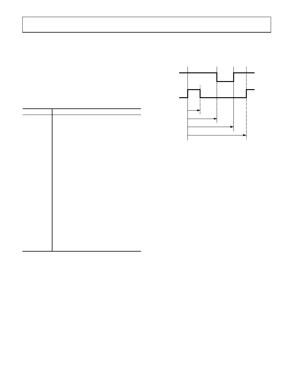
pair of PWM outputs (PWM0 and PWM1) is shown in Figure 26.
HIGH SIDE
(PWM0)
LOW SIDE
(PWM1)
PWM0COM2
PWM0COM1
PWM0COM0
PWM0LEN
07079-
020
Figure 26. PWM Timing
The PWM clock is selectable via PWMCON with one of the
following values: UCLK divided by 2, 4, 8, 16, 32, 64, 128, or
256. The length of a PWM period is defined by PWMxLEN.
The PWM waveforms are set by the count value of the 16-bit
timer and the compare registers contents, as shown with the
PWM0 and PWM1 waveforms in Figure 26.
The low-side waveform, PWM1, goes high when the timer
count reaches PWM0LEN, and it goes low when the timer
count reaches the value held in PWM0COM2 or when the
high-side waveform (PWM0) goes low.
The high-side waveform, PWM0, goes high when the timer
count reaches the value held in PWM0COM0, and it goes low
when the timer count reaches the value held in PWM0COM1.
PWMCON Control Register
Name:
PWMCON
Address:
0xFFFF0F80
Default value:
0x0012
Access:
Read and write
Function:
This is a 16-bit MMR that configures the
PWM outputs.
相关PDF资料 |
PDF描述 |
|---|---|
| VI-B2L-IW-F4 | CONVERTER MOD DC/DC 28V 100W |
| ATMEGA8535L-8JU | MCU AVR 8K ISP FLASH MEM 44-PLCC |
| VI-B2L-IW-F3 | CONVERTER MOD DC/DC 28V 100W |
| ATMEGA8535L-8PU | IC AVR MCU 8K 8MHZ 3V 40DIP |
| VI-B2L-IW-F2 | CONVERTER MOD DC/DC 28V 100W |
相关代理商/技术参数 |
参数描述 |
|---|---|
| ADUC70SMARTLINKRL7 | 制造商:Analog Devices 功能描述: |
| ADUC70TEL | 制造商:Analog Devices 功能描述:FLASH ARM +5-CH 12BIT ADC - Trays |
| ADUC70TEL-RL7 | 制造商:Analog Devices 功能描述: |
| ADUC7120BBCZ | 制造商:Analog Devices 功能描述:- Rail/Tube |
| ADUC7120BBCZ-RL | 制造商:Analog Devices 功能描述:- Tape and Reel |
发布紧急采购,3分钟左右您将得到回复。