- 您现在的位置:买卖IC网 > PDF目录11210 > ADUC7061BCPZ32-RL (Analog Devices Inc)IC MCU 16/32BIT 32KB 32LFCSP PDF资料下载
参数资料
| 型号: | ADUC7061BCPZ32-RL |
| 厂商: | Analog Devices Inc |
| 文件页数: | 40/108页 |
| 文件大小: | 0K |
| 描述: | IC MCU 16/32BIT 32KB 32LFCSP |
| 产品变化通告: | ADuC7060/1 Idd Specification Change 01/Feb/2010 |
| 设计资源: | USB Based Temperature Monitor Using ADuC7061 and an External RTD (CN0075) 4 mA-to-20 mA Loop-Powered Temperature Monitor Using ADuC7060/1 (CN0145) |
| 标准包装: | 5,000 |
| 系列: | MicroConverter® ADuC7xxx |
| 核心处理器: | ARM7 |
| 芯体尺寸: | 16/32-位 |
| 速度: | 10MHz |
| 连通性: | I²C,SPI,UART/USART |
| 外围设备: | POR,PWM,温度传感器,WDT |
| 输入/输出数: | 8 |
| 程序存储器容量: | 32KB(16K x 16) |
| 程序存储器类型: | 闪存 |
| RAM 容量: | 1K x 32 |
| 电压 - 电源 (Vcc/Vdd): | 2.375 V ~ 2.625 V |
| 数据转换器: | A/D 5x24b,8x24b,D/A 1x14b |
| 振荡器型: | 内部 |
| 工作温度: | -40°C ~ 125°C |
| 封装/外壳: | 32-VFQFN 裸露焊盘,CSP |
| 包装: | 带卷 (TR) |
第1页第2页第3页第4页第5页第6页第7页第8页第9页第10页第11页第12页第13页第14页第15页第16页第17页第18页第19页第20页第21页第22页第23页第24页第25页第26页第27页第28页第29页第30页第31页第32页第33页第34页第35页第36页第37页第38页第39页当前第40页第41页第42页第43页第44页第45页第46页第47页第48页第49页第50页第51页第52页第53页第54页第55页第56页第57页第58页第59页第60页第61页第62页第63页第64页第65页第66页第67页第68页第69页第70页第71页第72页第73页第74页第75页第76页第77页第78页第79页第80页第81页第82页第83页第84页第85页第86页第87页第88页第89页第90页第91页第92页第93页第94页第95页第96页第97页第98页第99页第100页第101页第102页第103页第104页第105页第106页第107页第108页
Data Sheet
ADuC7060/ADuC7061
Rev. D | Page 37 of 108
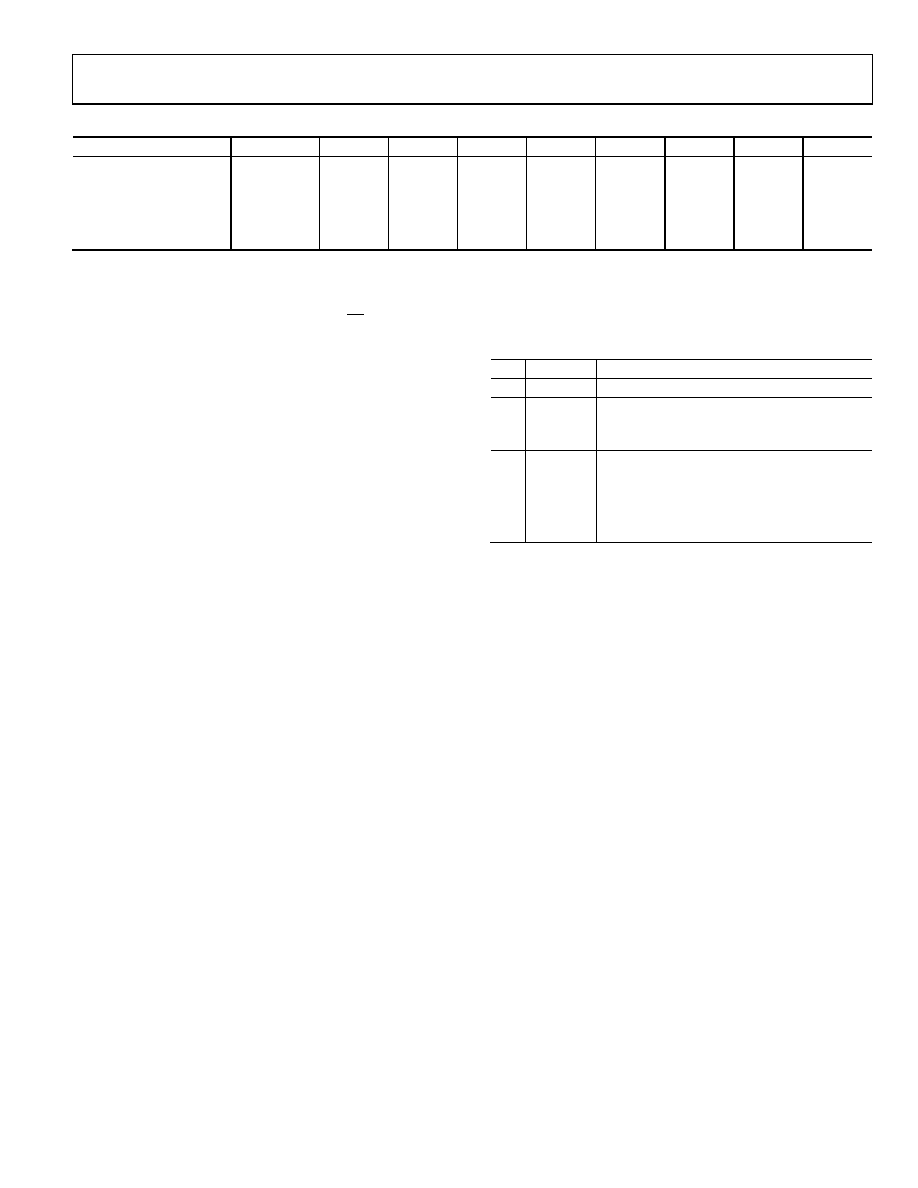
Table 34. Typical Current Consumption at 25°C in mA1
POWCON0[6:3]
Mode
CD = 0
CD = 1
CD = 2
CD = 3
CD = 4
CD = 5
CD = 6
CD = 7
1111
Active2
5.22
4.04
2.69
2.01
1.67
1.51
1.42
1.38
1110
Pause3
2.6
1.95
1.6
1.49
1.4
1.33
1.31
1.3
1100
Nap3
1.33
1.29
1000
Sleep3
0.085
0000
Stop3
0.055
1
All values listed in Table 34 have been taken with both ADCs turned off.
2
In active mode, GP0PAR bit 7 =1.
3
The values for pause, nap, sleep, and stop modes are measured with the NTRST pin low. To minimize IDD due to nTRST in all modes, set GP0PAR Bit 7 =1. This disables
the internal pull-down on the nTRST pin and means there is no ground path for the external pull-up resistor through the nTRST pin. By default, GP0PAR Bit 7 = 0,
therefore, setting this bit in user code will not affect the BMoperation.
Name:
PLLKEY1
Address:
0xFFFF0410
Default value: 0xXXXX
Access:
Write
Function:
When writing to the PLLCON register, the
value of 0xAA must be written to this register
in the instruction immediately before writing
to PLLCON.
Name:
PLLCON
Address:
0xFFFF0414
Default value:
0x00
Access:
Read and write
Function:
This register selects the clock input to the PLL.
Table 35. PLLCON MMR Bit Designations
Bit
Name
Description
7:3
Reserved
These bits must always be set to 0.
2
EXTCLK
Set this bit to 1 to select external clock input
from P2.0.
Clear this bit to disable the external clock.
1:0
OSEL
Oscillator selection bits.
[00] = internal 32,768 Hz oscillator.
[01] = internal 32,768 Hz oscillator.
[10] = external crystal.
[11] = internal 32,768 Hz oscillator.
Name:
PLLKEY2
Address:
0xFFFF0418
Default value:
0xXXXX
Access:
Write
Function:
When writing to PLLCON, the value of 0x55
must be written to this register in the
instruction immediately after writing to
PLLCON.
相关PDF资料 |
PDF描述 |
|---|---|
| VI-B2L-IW-F4 | CONVERTER MOD DC/DC 28V 100W |
| ATMEGA8535L-8JU | MCU AVR 8K ISP FLASH MEM 44-PLCC |
| VI-B2L-IW-F3 | CONVERTER MOD DC/DC 28V 100W |
| ATMEGA8535L-8PU | IC AVR MCU 8K 8MHZ 3V 40DIP |
| VI-B2L-IW-F2 | CONVERTER MOD DC/DC 28V 100W |
相关代理商/技术参数 |
参数描述 |
|---|---|
| ADUC70SMARTLINKRL7 | 制造商:Analog Devices 功能描述: |
| ADUC70TEL | 制造商:Analog Devices 功能描述:FLASH ARM +5-CH 12BIT ADC - Trays |
| ADUC70TEL-RL7 | 制造商:Analog Devices 功能描述: |
| ADUC7120BBCZ | 制造商:Analog Devices 功能描述:- Rail/Tube |
| ADUC7120BBCZ-RL | 制造商:Analog Devices 功能描述:- Tape and Reel |
发布紧急采购,3分钟左右您将得到回复。